High power supply rejection ratio and low temperature drift band-gap reference voltage source
A technology of high power supply rejection ratio and reference voltage source, which is applied in the direction of adjusting electrical variables, control/regulation systems, instruments, etc., and can solve problems that cannot meet the temperature stability requirements of the reference voltage source
- Summary
- Abstract
- Description
- Claims
- Application Information
AI Technical Summary
Problems solved by technology
Method used
Image
Examples
Embodiment Construction
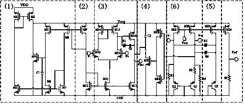
[0071] like figure 1 As shown, the high power supply rejection ratio low-temperature drift bandgap reference voltage source includes: DC voltage source Vdd, pre-regulation circuit (1), bias circuit (2), operational amplifier (3), start-up circuit (4), temperature compensation Circuit (5), bandgap reference core circuit (6).
[0072] Wherein, the pre-adjustment circuit (1) includes: MOS field effect transistors M1, M2, M3, M4, M5, M6, M7, M8 and capacitor C1; wherein said transistors M1, M2, M5, M8 are PMOS field effect transistors Effect transistors; the transistors M3, M4, M6, and M7 are NMOS field effect transistors.
[0073] The sources of the PMOS field effect transistors M1 and M2 are connected and connected to the power supply voltage (VDD); the gate of the PMOS field effect transistor M1 is connected to the drain; the PMOS field effect transistor M1 is connected to the gate of M2; the PMOS field effect transistor M1 is connected to the gate of M2; Field effect transis...
PUM
 Abstract
Description
Claims
Application Information
 - R&D Engineer
- R&D Manager
- IP Professional
- Industry Leading Data Capabilities
- Powerful AI technology
- Patent DNA Extraction
Browse by: Latest US Patents, China's latest patents, Technical Efficacy Thesaurus, Application Domain, Technology Topic, Popular Technical Reports.
© 2024 PatSnap. All rights reserved.Legal|Privacy policy|Modern Slavery Act Transparency Statement|Sitemap|About US| Contact US: help@patsnap.com


