OLED display panel and manufacturing method thereof

A technology for display panels and manufacturing methods, applied in chemical instruments and methods, manufacturing tools, lamination auxiliary operations, etc., can solve the problems of expensive equipment, affecting the process, and burnt electrodes 230, so as to reduce the generation of particulate matter and protect burns Damage, the effect of ensuring the encapsulation effect

Inactive Publication Date: 2018-08-10
WUHAN CHINA STAR OPTOELECTRONICS SEMICON DISPLAY TECH CO LTD
View PDF4 Cites 11 Cited by
  • Summary
  • Abstract
  • Description
  • Claims
  • Application Information

AI Technical Summary

Problems solved by technology

[0012] The first question is: if Figure 11 As shown, in step 5 of the above-mentioned frit glue packaging process, in order to ensure that the frit glue 300 is completely cured, the diameter of the laser beam 950 (laser beam) needs to be larger than the width of the frit glue 300, but the laser beam wider than the frit glue 300 will pass through the package When the cover plate 100 is irradiated on the electrode 230 of the OLED substrate 200, it is easy to cause the electrode 230 of the OLED substrate 200 to burn, so that the electrode 230 is disconnected, and the OLED device 220 fails;
However, this method also has the following problems: first, this method needs to be supported by a sophisticated alignment system, the equipment is expensive, and alignment abnormalities are prone to occur; second, the laser light blocked by the mask plate 850 will be reflected back On the laser head 810 (laser head), causing the laser head 810 to be burned and damaged
[0014] The second question is: if figure 2 As shown, frit glue 300 is trapezoidal after being baked in step 2, that is, it includes a thick layer area in the middle and thin layer areas on both sides, as shown in Figure 7 As shown, in the process of laser scanning the frit glue 300, since the energy of different regions in the laser beam 950 (laser beam) is uniform, the thin layer regions on both sides of the frit glue 300 will be burnt by too much laser energy , affecting the encapsulation effect, and the particles produced by burning will also affect the subsequent process

Method used


Image

  • OLED display panel and manufacturing method thereof
  • OLED display panel and manufacturing method thereof
  • OLED display panel and manufacturing method thereof

Examples


Embodiment Construction

[0078] In order to further illustrate the technical means adopted by the present invention and its effects, the following describes in detail in conjunction with preferred embodiments of the present invention and accompanying drawings.

[0079] see Figure 13 , the invention provides a method for manufacturing an OLED display panel, comprising the following steps:

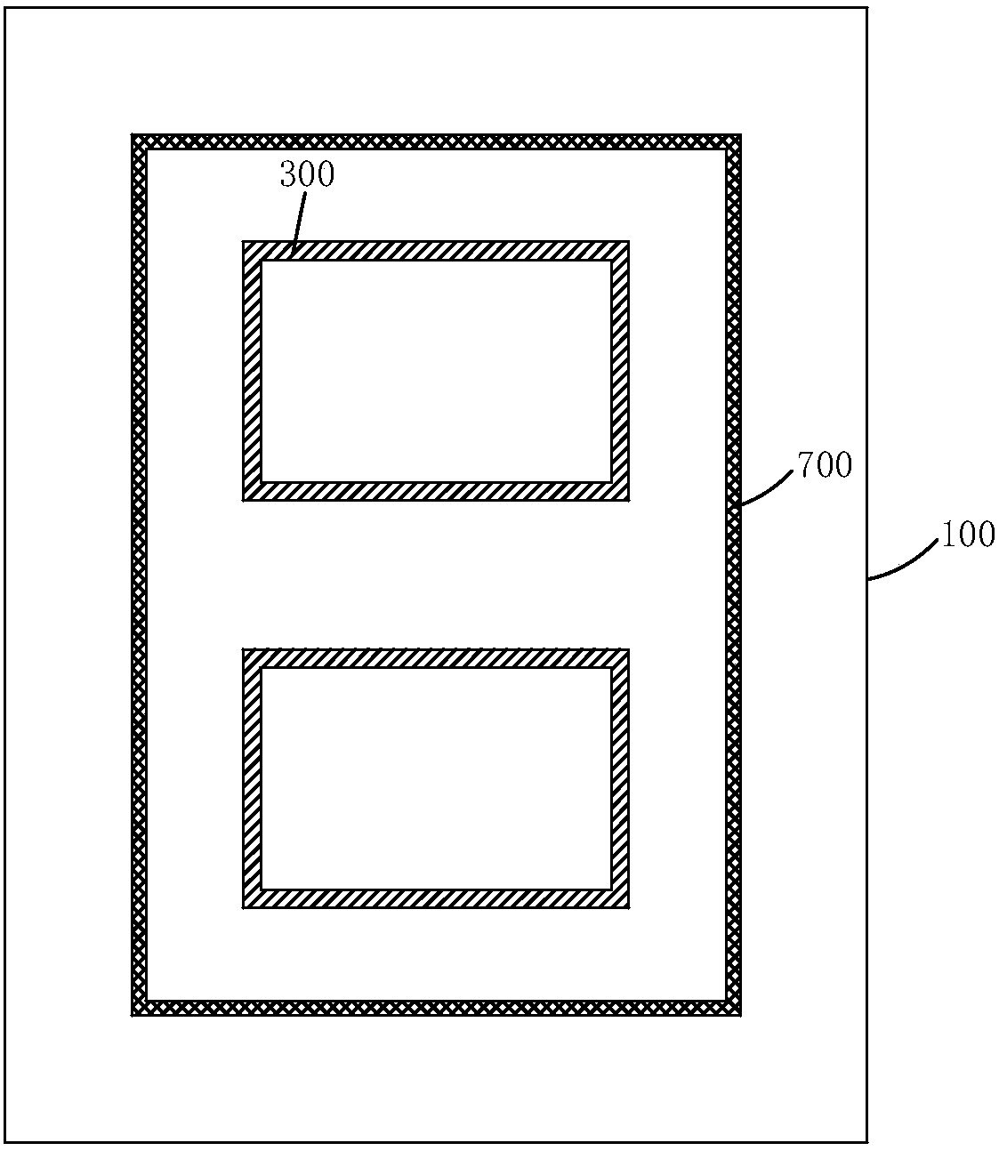
[0080] Step 1, such as Figure 14 to Figure 17 As shown, a package cover 10 is provided, and the package cover 10 includes a cover body 11 and a first light-shielding film 51 and a second light-shielding film 52 arranged on the cover body 11; One or more sealant coating areas 40, the sealant coating area 40 includes a thick sealant area 43 and a first thin sealant area 41 and a second thin sealant area 42 located on both sides of the thick sealant area 43 ; The first light-shielding film 51 and the second light-shielding film 52 are respectively arranged on both sides of the frame rubber thick area 43;

[0081] ...


PUM


Abstract

The invention provides an OLED display panel and a manufacturing method thereof. According to the manufacturing method of the OLED display panel, a light-shielding film is arranged on a packaging cover plate, and the laser can be prevented from irradiating electrodes on an OLED substrate in the laser scanning process of a frame adhesive. In this way, electrodes are effectively protected. Meanwhile, the part of the light-shielding film, overlapped with the film region of the frame adhesive, has a gradually-reduced light transmittance, so that the film region of the frame adhesive can be prevented from being burnt by the excessive laser energy. The packaging effect is fully guaranteed, and the generation of particulate matters is reduced. In addition, the surface of the light-shielding film,irradiated by the laser, is set to be a frosted surface, so that the laser irradiated on the light-shielding film can generate the diffuse reflection. As a result, the laser is prevented from being directly reflected to a laser head, so that the laser head is protected from being damaged by burns. The OLED display panel is prepared by adopting the above manufacturing method of the OLED display panel, so that the OLED display panel is good in packaging effect and high in production yield.

Description

technical field [0001] The invention relates to the field of display technology, in particular to an OLED display panel and a manufacturing method thereof. Background technique [0002] Organic Light Emitting Display (OLED) is a new generation of displays. OLED devices usually include a cathode, an anode, and an organic film sandwiched between the cathode and the anode. After applying a voltage between the cathode and the anode, the organic The film will glow. Compared with liquid crystal displays, OLED displays have many advantages such as self-illumination, fast response, wide viewing angle, and saturated colors. [0003] The water and oxygen in the air will oxidize the active wave metal of the cathode of the OLED device, and chemically react with the organic material, which will cause the OLED device to fail. Therefore, effective encapsulation of OLED devices to fully isolate OLED devices from water and oxygen is crucial to prolonging the life of OLED devices. [0004]...

Claims


Application Information

Patent Timeline
Patent Type & Authority Applications(China)
IPC IPC(8): H01L51/52H01L51/56
CPCH10K50/841H10K50/8426H10K71/00B32B37/12B32B38/0008B32B2037/1253B32B2457/206B23K26/352B23K26/38B32B38/0004H10K59/12H10K59/1201H10K71/851
Inventor 余威
Owner WUHAN CHINA STAR OPTOELECTRONICS SEMICON DISPLAY TECH CO LTD
Why Eureka
Try Eureka