A kind of 3D through-hole superstructure LED chip and preparation method thereof

A technology of LED chips and superstructures, applied in semiconductor devices, electrical components, circuits, etc., can solve the problems of lithography process pattern alignment, insulation problems, the actual protection effect of the protective layer metal and stress regulation, etc., to achieve excellent Super-current drive capability, improved current distribution uniformity, and high yield

Active Publication Date: 2019-11-12
HEYUAN CHOICORE PHOTOELECTRIC TECH CO LTD
View PDF3 Cites 0 Cited by
  • Summary
  • Abstract
  • Description
  • Claims
  • Application Information

AI Technical Summary

Problems solved by technology

[0003] Although the 3D through-hole superstructure LED chip has so many advantages, there are still the following defects: the insulation problem between the p-electrode metal and the n-electrode metal; the pattern alignment problem of the photolithography process in the hole manufacturing process; Protection effect and stress regulation; hole side wall anti-leakage protection; hole diameter, hole shape, hole spacing and distribution design and other problems

Method used


Image

  • A kind of 3D through-hole superstructure LED chip and preparation method thereof
  • A kind of 3D through-hole superstructure LED chip and preparation method thereof
  • A kind of 3D through-hole superstructure LED chip and preparation method thereof

Examples


Embodiment 1

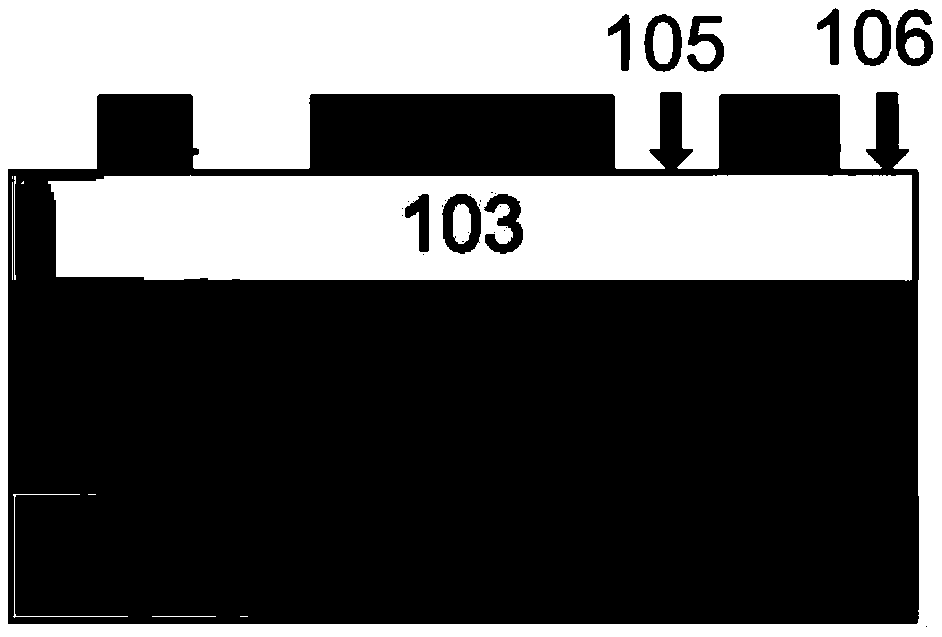
[0067] Such as Picture 11 As shown, a 3D through-hole superstructure LED chip includes a second insulating layer 115, an n-GaN layer 101 (n-type doped GaN film), an InGaN / GaN multiple quantum well layer 102, and a p-GaN layer stacked in sequence 103 (p-type doped GaN film), mirror layer 104, mirror protection layer 107, first insulating layer 111, first bonding layer 114, second bonding layer 201, bonding substrate 200, and back gold layer 202; the mirror layer 104 is provided with a first opening 105 and a second opening 106, the second opening 106 is located at the edge of the mirror layer 104; the mirror protection layer 107 is provided on the mirror layer 104 and covers the first The bottom and sidewalls of the opening 105 and the bottom and sidewalls of the second opening 106 are covered; the mirror protection layer 107 is provided with a third opening 108 and a walkway 109, the third opening 108 and the first opening 105 Passing through up and down, the walkway 109 is ci...

Embodiment 2

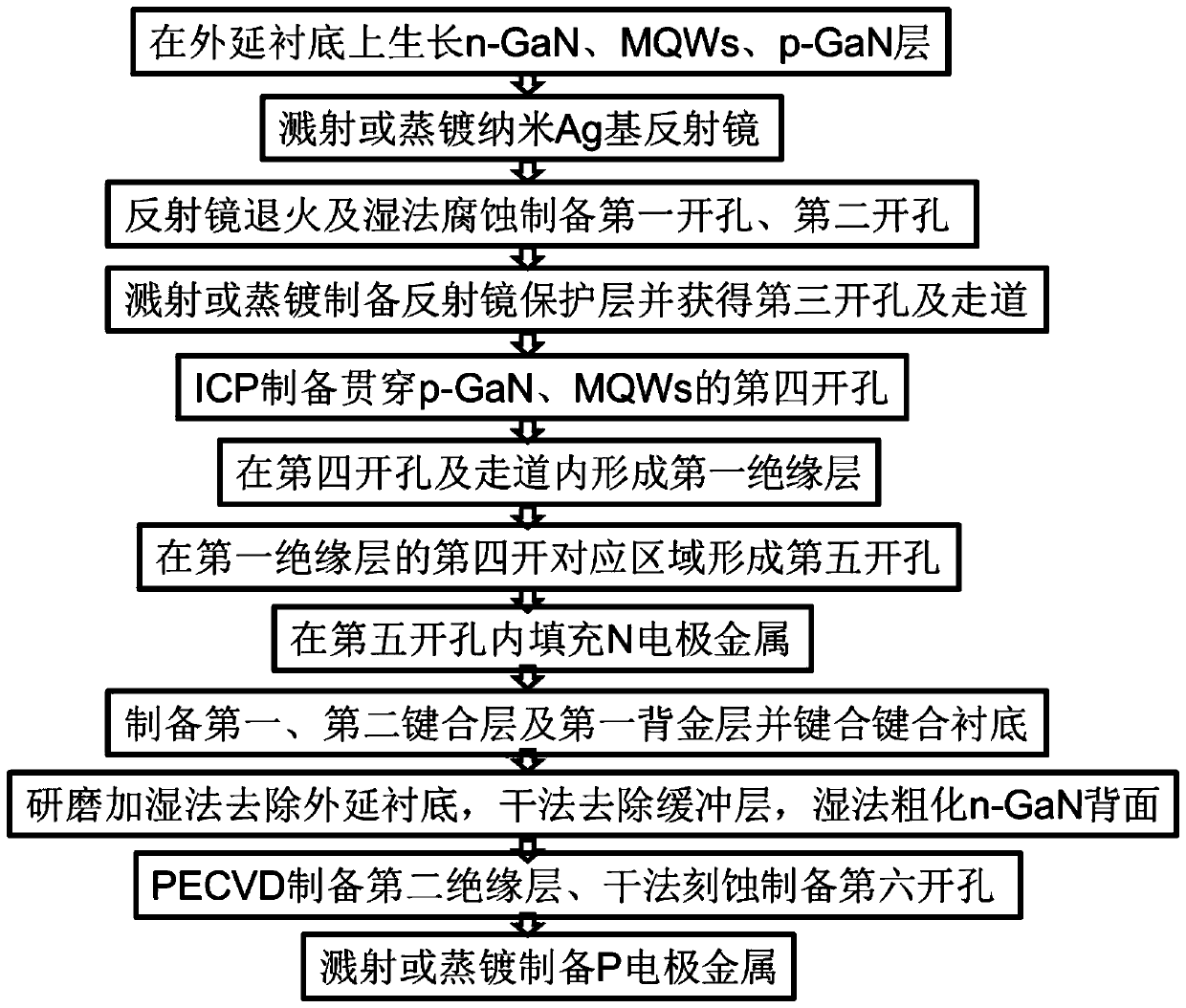
[0077] Such as Figure 1-11 As shown, a method for preparing a 3D through-hole superstructure LED chip includes:

[0078] The epitaxial growth step: take the epitaxial substrate, and sequentially grow the n-GaN layer 101, the InGaN / GaN multiple quantum well layer 102 and the p-GaN layer 103 on the epitaxial substrate;

[0079] Evaporation and hole-opening step: vapor-deposit a mirror layer 104 on the p-GaN layer 103, and after high-temperature annealing, a first hole 105 and a second hole 106 are opened on the mirror layer 104, and the second hole 106 is located in the reflective layer. The edge of the mirror layer 104;

[0080] Step of preparing a mirror protection layer 107: preparing a mirror protection layer 107 on the mirror layer 104, and the mirror protection layer 107 covers the bottom and side walls of the first opening 105 and the bottom and sides of the second opening 106 Wall; Next, a third opening 108 and aisle 109 are provided on the mirror protection layer 107, the t...


PUM

PropertyMeasurementUnit
thicknessaaaaaaaaaa
thicknessaaaaaaaaaa
thicknessaaaaaaaaaa

Abstract

The invention discloses a silicon-based 3D through-hole super-structure LED chip and a preparation method thereof. The preparation method comprises that an n-GaN layer, an InGaN / GaN multi-quantum welllayer and a p-GaN layer are grown on an epitaxial substrate successively, a reflector layer and a reflector protection layer are prepared, holes are formed, an insulating layer is prepared, and N electrode metal filling the holes and bonding-layer metal are prepared; a growth substrate is peeled, an MESA channel and a PA layer are prepared, and P electrode metal is prepared; and the complete silicon-based LED chip with the vertical 3D hole structure is prepared. The 3D through hole super structure has advantages of a vertical linear structure, and converts a 2D current expansion capability ofthe linear structure into a 3D current expansion capability, the current distribution uniformity is greatly improved, and the luminous efficiency is improved greatly.

Description

Technical field [0001] The invention relates to the technical field of LED manufacturing, in particular to a 3D through-hole superstructure LED chip and a preparation method thereof. Background technique [0002] With the gradual application of LEDs in the lighting field, the market has higher and higher requirements for the luminous efficiency of white light LEDs. The GaN-based vertical linear structure LED chips emerging in the LED market are capable of withstanding single-sided light emission and good heat dissipation. A series of advantages such as high current injection and a fraction of the cost of a formal structure are gradually replacing sapphire-based horizontal structure LED chips and becoming the first choice in the high-power LED market. However, the vertical linear structure LED also has its shortcomings. First, because its N electrode is placed on the light-emitting surface, there is a serious problem of electrode blocking light; second, the current expansion capab...

Claims


Application Information

Patent Timeline
Patent Type & Authority Patents(China)
IPC IPC(8): H01L33/60H01L33/62H01L33/00
CPCH01L33/0075H01L33/0095H01L33/60H01L33/62
Inventor 李国强
Owner HEYUAN CHOICORE PHOTOELECTRIC TECH CO LTD
Why Eureka
Try Eureka