Light-emitting diode and manufacturing method thereof

A technology of light-emitting diodes and light-emitting layers, which is applied to semiconductor devices, electrical components, circuits, etc., can solve the problems of LED light-emitting efficiency decline, reduce Ag reflectivity, etc., improve the uniformity of current distribution, suppress the sudden drop of efficiency, and improve the current distribution effect

Active Publication Date: 2021-04-13
SHENZHEN INST OF WIDE BANDGAP SEMICON
View PDF7 Cites 0 Cited by
  • Summary
  • Abstract
  • Description
  • Claims
  • Application Information

AI Technical Summary

Problems solved by technology

For LED chips with a flip-chip structure, Ag can usually be used as the p-type ohmic contact and reflector, but the formation of ohmic contact between Ag and p-type GaN requires the introduction of high-temperature annealing process, which will reduce the reflectivity of Ag and cause The decline of LED luminous efficiency
It is also possible to use the method of coating a layer of Ag reflector on the ITO after the Omni conductive ITO material and p-type gallium nitride form a good ohmic contact, and separate the ohmic contact and the reflector process, but due to the ITO material itself It will also absorb light, which will also cause a decrease in the light output efficiency of the LED.

Method used


Image

  • Light-emitting diode and manufacturing method thereof
  • Light-emitting diode and manufacturing method thereof
  • Light-emitting diode and manufacturing method thereof

Examples


Embodiment Construction

[0019] The following will clearly and completely describe the technical solutions in the embodiments of the present application with reference to the drawings in the embodiments of the present application. Obviously, the described embodiments are only some of the embodiments of the present application, not all of them. Based on the embodiments in this application, all other embodiments obtained by persons of ordinary skill in the art without making creative efforts belong to the scope of protection of this application.

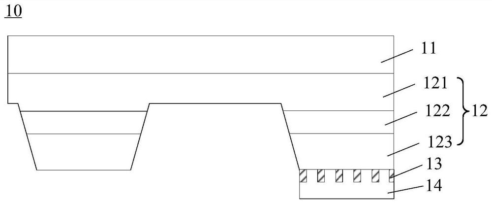
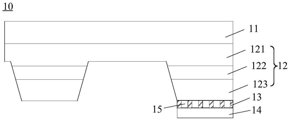
[0020] For vertical or flip-chip light-emitting diodes, the prior art generally uses an Ag layer as a reflector, and annealing the Ag layer makes the Ag layer both function as a reflector and an ohmic contact pattern. After the evaporation of the metal electrode on the P surface is completed, a planar electrode-mirror structure will be formed, and this region will become a surface current injection region. The current density of the above structure gradually d...


PUM

PropertyMeasurementUnit
Thicknessaaaaaaaaaa

Abstract

The invention relates to the field of light emitting diodes, and particularly discloses a light emitting diode and a manufacturing method thereof. The light emitting diode comprises: a substrate; a light-emitting epitaxial layer comprising a first semiconductor layer, an active light-emitting layer and a second semiconductor layer which are sequentially stacked on one side of the substrate; a plurality of ohmic contact patterns arranged on one side, deviating from the active light-emitting layer, of the first semiconductor layer or the second semiconductor layer at intervals in a dot matrix mode; and a reflector layer positioned on one side, deviating from the active light-emitting layer, of the plurality of ohmic contact patterns and covering the plurality of ohmic contact patterns and the first semiconductor layer or the second semiconductor layer between the plurality of ohmic contact patterns. By means of the mode, current distribution can be effectively improved, the current distribution uniformity is improved, the efficiency sudden drop effect under large current is restrained, and the reflectivity of the reflector is improved.

Description

technical field [0001] The present application relates to the field of light-emitting diodes, in particular to a light-emitting diode and a manufacturing method thereof. Background technique [0002] A light emitting diode (Light Emitting Diode, LED) is a semiconductor element that can convert electric current into light in a specific wavelength range. Light-emitting diodes can be widely used as light sources in the field of lighting because of their advantages such as high brightness, low operating voltage, low power consumption, easy matching with integrated circuits, simple driving, and long life. [0003] LEDs generally include a first semiconductor layer, a light emitting epitaxial layer and a second semiconductor layer. When voltage is applied across the LED, holes and electrons will recombine in the light-emitting epitaxial layer and emit photons. One of the problems faced by LEDs in the application process is their light extraction efficiency. Since photons can on...

Claims


Application Information

Patent Timeline
IPC IPC(8): H01L33/38H01L33/40H01L33/46H01L33/00
CPCH01L33/387H01L33/405H01L33/46H01L33/0075H01L2933/0016
Inventor 蒋振宇闫春辉
Owner SHENZHEN INST OF WIDE BANDGAP SEMICON
Why Eureka
Try Eureka