Semiconductor light emitting device and manufacturing method thereof

A light-emitting device and semiconductor technology, applied in semiconductor devices, electrical components, circuits, etc., can solve the problems of reducing the working life of the device, limiting the rated power of the device, and breakdown of the light-emitting device, so as to achieve the suppression of current edge effect and good electrical connection Effect

Active Publication Date: 2013-01-23
INST OF SEMICONDUCTORS - CHINESE ACAD OF SCI
View PDF2 Cites 3 Cited by
  • Summary
  • Abstract
  • Description
  • Claims
  • Application Information

AI Technical Summary

Problems solved by technology

The current edge effect can easily cause local overheating and breakdown of the light-emitting device, which will reduce the working life of the device and limit the rated power of the device
In addition, the current edge effect will greatly reduce the luminous efficiency

Method used


Image

  • Semiconductor light emitting device and manufacturing method thereof
  • Semiconductor light emitting device and manufacturing method thereof
  • Semiconductor light emitting device and manufacturing method thereof

Examples


Embodiment Construction

[0027] In order to make the object, technical solution and advantages of the present invention clearer, the present invention will be described in further detail below in conjunction with specific embodiments and with reference to the accompanying drawings.

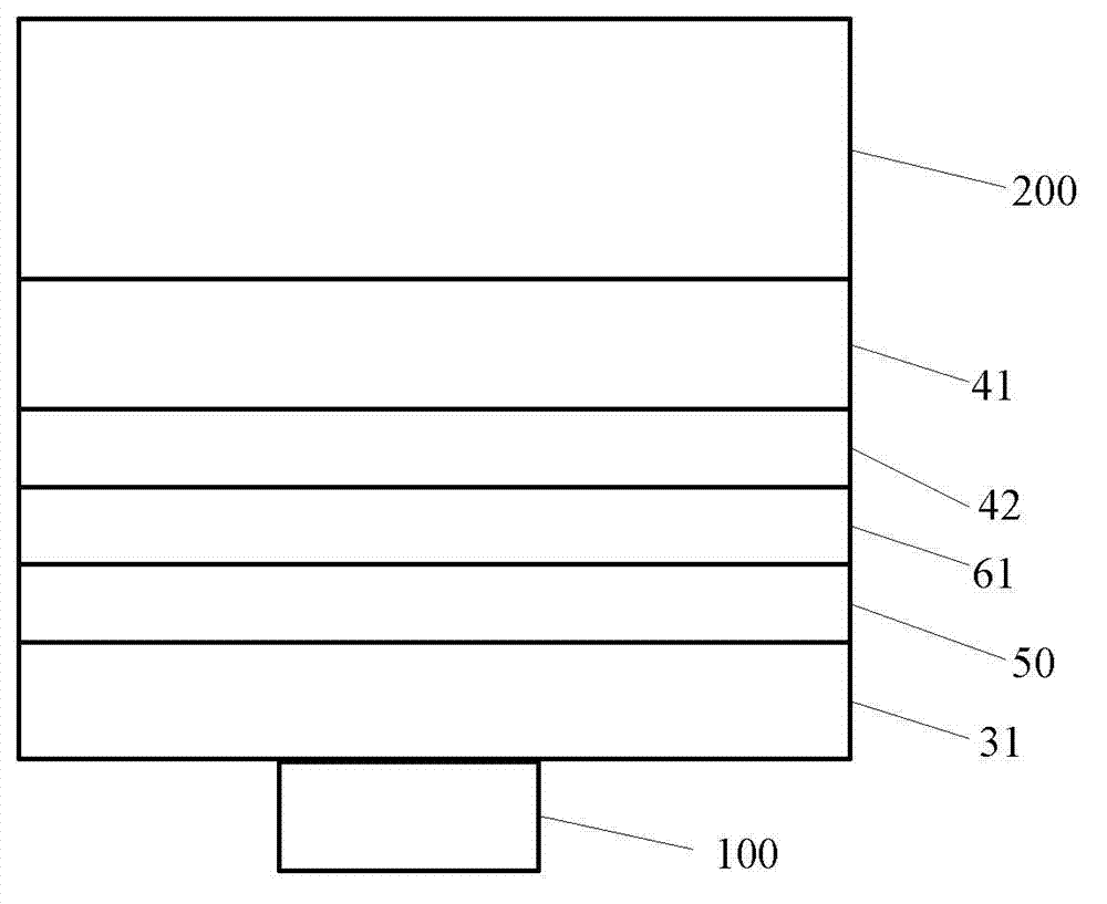
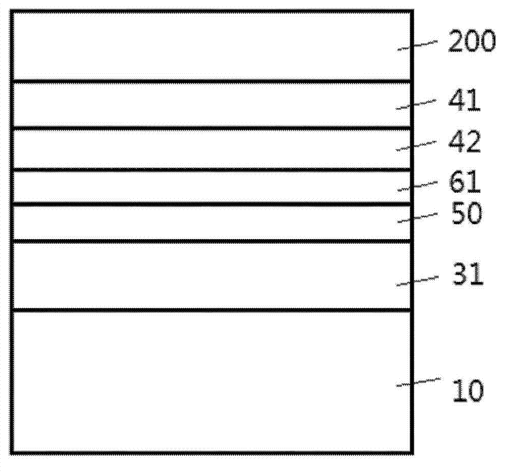
[0028] It should be noted that, in the drawings or descriptions of the specification, similar or identical parts all use the same figure numbers. Implementations not shown or described in the accompanying drawings are forms known to those of ordinary skill in the art. Additionally, while illustrations of parameters including particular values ​​may be provided herein, it should be understood that the parameters need not be exactly equal to the corresponding values, but rather may approximate the corresponding values ​​within acceptable error margins or design constraints. In addition, the directional terms mentioned in the following embodiments, such as "upper", "lower", "front", "rear", "left", "right", etc., are only re...


PUM


Abstract

The invention provides a semiconductor light emitting device and a manufacturing method thereof. The semiconductor light emitting device comprises a second electrode, a first semiconductor layer of a first doped type, an active layer, a second semiconductor layer of a second doped type, a first degenerate semiconductor layer of a first doped type, a second degenerate semiconductor layer of a second doped type, and a first electrode electrically connected with the second degenerate semiconductor layer, wherein the first semiconductor layer of the first doped type is electrically connected with the second electrode; the active layer is formed on the first semiconductor layer; the second semiconductor layer of the second doped type is formed on the active layer; the first degenerate semiconductor layer of the first doped type is formed on the second semiconductor layer; and the second degenerate semiconductor layer of the second doped type is formed on the first degenerate semiconductor layer. According to the invention, a positively biased tunneling pn junction is inserted into the semiconductor light emitting device, thus the current distribution uniformity of a power type semiconductor light emitting device is greatly improved, and the current crowing effect is solved.

Description

technical field [0001] The invention relates to the technical field of semiconductors, in particular to a semiconductor light emitting device and a manufacturing method thereof. Background technique [0002] With the development of semiconductor technology, the application of semiconductor light emitting devices is becoming more and more extensive. The so-called semiconductor light-emitting devices, including semiconductor light-emitting diodes and laser diodes, are devices based on compound semiconductor materials and processed by epitaxy, die fabrication, and subsequent packaging. They are widely used in information processing and communication and other technical fields. [0003] For a semiconductor light-emitting device, the electrode area of ​​its light-emitting surface always only occupies a small part of its corresponding working area, and the current injected by the device tends to be concentrated near the electrode and cannot be effectively spread throughout the dev...

Claims


Application Information

Patent Timeline
Patent Type & Authority Applications(China)
IPC IPC(8): H01L33/14H01L33/04H01L33/00
Inventor 郭恩卿伊晓燕王国宏刘志强
Owner INST OF SEMICONDUCTORS - CHINESE ACAD OF SCI
Why Eureka
Try Eureka