led device structure

A technology for LED devices and material layers, applied in semiconductor devices, electrical components, circuits, etc., can solve the problems of occupying light-emitting area, reducing the light-emitting brightness of LED devices, and lack of N-layer GaN current expansion, etc., to increase uniformity and efficiency. Effect

Inactive Publication Date: 2018-05-29
EPILIGHT TECH
View PDF4 Cites 0 Cited by
  • Summary
  • Abstract
  • Description
  • Claims
  • Application Information

AI Technical Summary

Problems solved by technology

[0011] In the above-mentioned LED devices, the efficiency of the current is mainly expanded by adding linear electrodes, and the uniformity of the current distribution of the device is increased. However, in this way, the increased linear electrodes will occupy the light-emitting area, which will reduce the luminous brightness of the LED device to a certain extent.
In addition, as shown above, in the prior art, the application of the insulating layer is mainly limited to the P-type GaN layer in the LED device to adjust and expand the current distribution in the P-type GaN layer, but there is no effective N-layer GaN layer. Current Extended Technology

Method used


Image

  • led device structure
  • led device structure
  • led device structure

Examples


Embodiment Construction

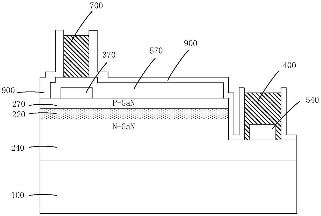
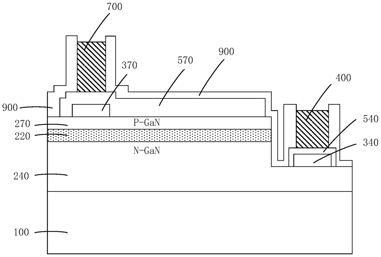
[0052]In traditional technology, the LED device structure is generally based on the N-type GaN layer and the P-type GaN layer on the sapphire substrate from bottom to top, and the quantum well layer formed between the N-type GaN layer and the P-type GaN layer. . Since the P-type GaN layer is closer to the surface, and the quantum well layer is the main light-emitting surface of the LED device, generally the insulating layer under the metal layer in the electrode is mainly added on the P-type GaN layer to adjust and expand the P-type GaN layer. Current distribution in the GaN layer. However, only a part of the N-type GaN layer is exposed, and it is located under the quantum well layer. Therefore, in terms of improving the luminous brightness of LED devices, people do not pay much attention to the N-type GaN layer.

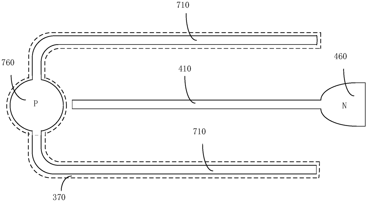
[0053] in the opposite figure 2 When a voltage is applied to the electrode structure shown in , a voltage signal is provided to the P-block metal electrode part ...


PUM


Abstract

The invention provides an LED device structure. The LED device structure sequentially comprises a semiconductor substrate, a P-type semiconductor layer, a luminous layer and an N-type semiconductor material layer, wherein a part of the N-type semiconductor material layer exposes. A P-electrode and an N-electrode which are separated are respectively formed on the P-type semiconductor material layer and the N-type semiconductor material layer and respectively comprise an insulating layer, a transparent conductive layer and a metal layer, wherein the metal layer comprises the P-block-shaped metal electrode portion and P-linear metal electrode portion which are connected mutually and a N-block-shaped metal electrode portion and N-linear metal electrode portion which are connected mutually. The N-block-shaped metal electrode portion extends towards the direction of the P-block-shaped metal electrode portion from the N-linear metal electrode portion, and the insulating layer of the N-electrode is located right under the N-linear metal electrode portion. By arranging the insulating layer right under the N-linear metal electrode portion, the distribution uniformity of current in an N-type GaN layer is improved, and the brightness of an LED device is further improved.

Description

technical field [0001] The invention relates to the technical field of semiconductors, in particular to an LED device structure. Background technique [0002] Light Emitting Diode (Light Emitting Diode, abbreviated as LED) has excellent characteristics such as long life, shock resistance, shock resistance, high efficiency and energy saving, and has extremely broad application prospects in image display, signal indication, lighting and basic research. GaN-based light-emitting diodes have developed rapidly in recent years, and LED chip technology is becoming more and more mature. Improving the brightness and yield of LED chips is the most important task at this stage. [0003] Existing LED device structures such as Figure 1 to Figure 2 shown, where figure 1 structure shown as a cross-section of the LED, figure 2 Shown is a top view of the electrode structure of the LED device. [0004] Such as figure 1 As shown in , the LED device structure includes a semiconductor sub...

Claims


Application Information

Patent Timeline
Patent Type & Authority Patents(China)
IPC IPC(8): H01L33/38H01L33/02
CPCH01L33/0075H01L33/14H01L33/38H01L2933/0016
Inventor 刘亚柱吕振兴齐胜利
Owner EPILIGHT TECH
Why Eureka
Try Eureka