AlGaInP semiconductor laser with superlattice limiting layer
A confinement layer and superlattice technology, which is applied in the field of AlGaInP semiconductor lasers, can solve the problems of easy diffusion and high doping of Mg atoms, and achieve the effect of increasing the effective barrier, reducing the probability, and preventing hot electrons from leaking into the P-type region
- Summary
- Abstract
- Description
- Claims
- Application Information
AI Technical Summary
Problems solved by technology
Method used
Image
Examples
Embodiment
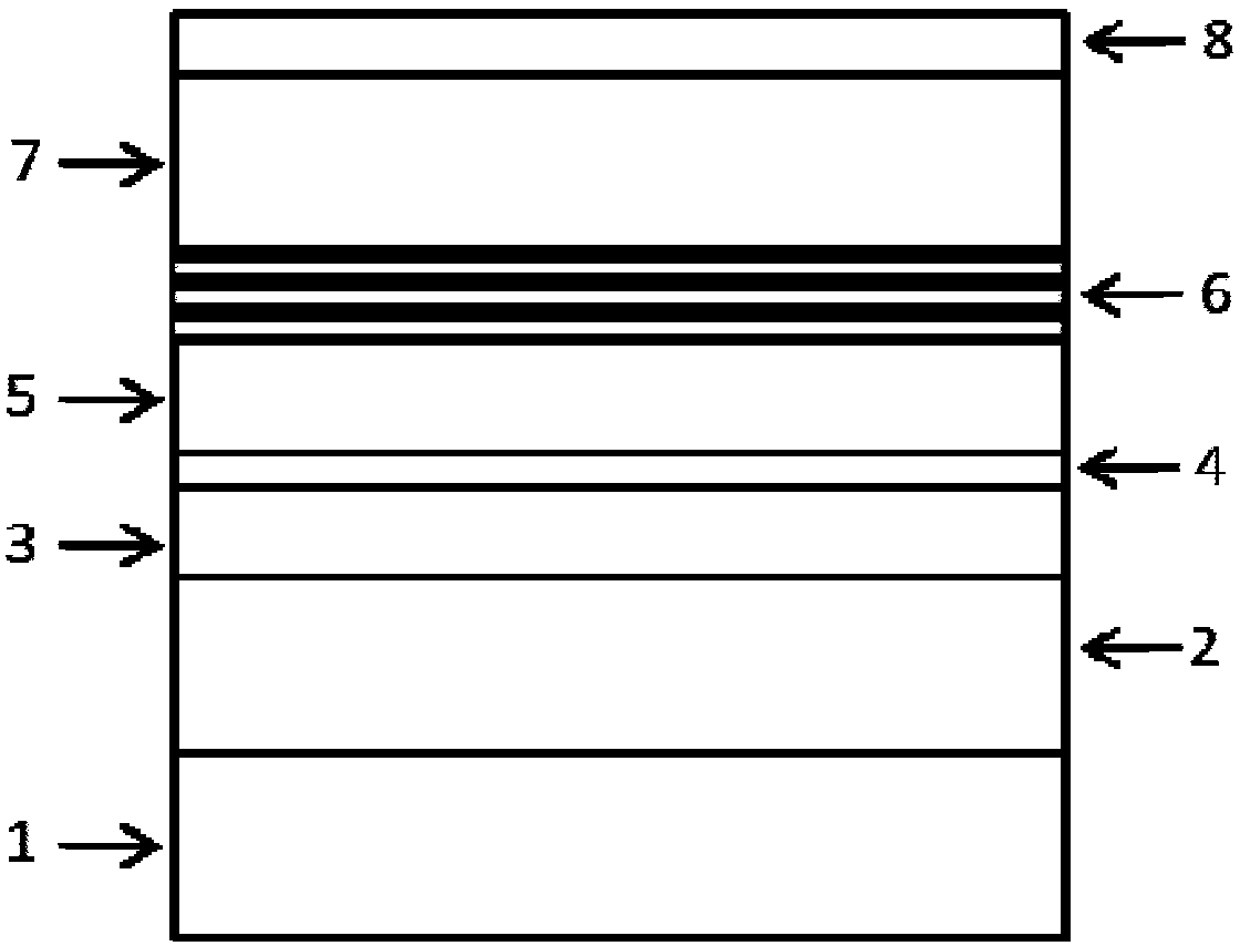
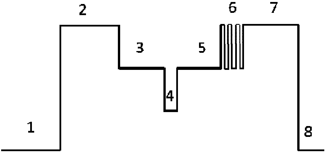
[0031] like figure 1 As shown, an AlGaInP semiconductor laser with a superlattice confinement layer comprises, from bottom to top, a substrate 1, a lower confinement layer 2, a lower waveguide layer 3, a quantum well layer 4, an upper waveguide layer 5, and a first upper confinement layer 6. The second upper confinement layer 7 and the ohmic contact layer 8 .
[0032] The substrate 1 is an N-type GaAs (100) single wafer with a biased crystal orientation, the off-angle is 10°, the N-type dopant material is Si, and the doping concentration is 3×10 18 cm -3 .
[0033] The lower confinement layer 2 is N-type (Al 0.7 Ga 0.3 ) 0.5 In 0.5 P, N type doping material is Si, doping concentration is 8×10 17 cm -3 , with a thickness of 1200nm.
[0034] The lower waveguide layer 3 is non-doped (Al 0.5 Ga 0.5 ) 0.5 In 0.5 P, with a thickness of 100 nm.
[0035] Quantum well layer 4 is Ga 0.45 In 0.55 P, the thickness is 10nm, and the lasing wavelength is 650nm.
[0036] The...
PUM
 Abstract
Description
Claims
Application Information
 - R&D
- Intellectual Property
- Life Sciences
- Materials
- Tech Scout
- Unparalleled Data Quality
- Higher Quality Content
- 60% Fewer Hallucinations
Browse by: Latest US Patents, China's latest patents, Technical Efficacy Thesaurus, Application Domain, Technology Topic, Popular Technical Reports.
© 2025 PatSnap. All rights reserved.Legal|Privacy policy|Modern Slavery Act Transparency Statement|Sitemap|About US| Contact US: help@patsnap.com


