A kind of neodymium indium zinc oxide thin film transistor and its preparation method

A technology of oxide thin film and transistor, which is applied in the direction of transistor, semiconductor/solid-state device manufacturing, semiconductor device, etc., can solve the problems of difficult to realize MOSTFT, carrier mobility reduction, unfavorable flexible display devices, etc., and achieve short time consumption, The effect of high mobility and simple process

Active Publication Date: 2021-05-14
SOUTH CHINA UNIV OF TECH
View PDF2 Cites 0 Cited by
  • Summary
  • Abstract
  • Description
  • Claims
  • Application Information

AI Technical Summary

Problems solved by technology

However, the doping of Ga elements also greatly reduces the mobility of carriers, and it will be difficult to achieve higher performance MOS TFTs only by using low-temperature or room-temperature processes.
This is not conducive to the development of higher performance flexible display devices with limited process temperature

Method used


Image

  • A kind of neodymium indium zinc oxide thin film transistor and its preparation method
  • A kind of neodymium indium zinc oxide thin film transistor and its preparation method
  • A kind of neodymium indium zinc oxide thin film transistor and its preparation method

Examples


Embodiment

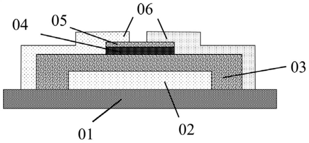
[0027]A method of preparing a rye indium zinc oxide thin film transistor in this embodiment, the specific steps are as follows:

[0028](1) The 300 nm Al metal film is deposited on the glass substrate by a DC sputtering method at room temperature and patterning with a mask plate.

[0029](2) Allowance of 200 nm of 200 nm in the gate to Al by anode oxidation method2O3As the gate insulating layer;

[0030](3) Nd-IZO semiconductor active layer was prepared by radio frequency sputtering method, and each material ratio in the indium zinc oxide (ND)2O3: In2O3: ZnO wt.%) Is 1: 62.5: 36.5 wt.%. The total pressure of the sputter is 3 mTorr, the sputter atmosphere is Ar / O2= 100 / 5 mixed gas, RF power power is 60 W, the sputtering time is 215 s; the thickness of the Nd-IZO semiconductor active layer is about 9 nm;

[0031](4) Preparation of ultra-thin Al by radio frequency sputtering at room temperature2O3The passivation layer, the sputtering total pressure is 1 mTorr, the sputtering atmosphere is a pure...


PUM

PropertyMeasurementUnit
thicknessaaaaaaaaaa
thicknessaaaaaaaaaa
widthaaaaaaaaaa

Abstract

The invention belongs to the technical field of display devices, and discloses a neodymium indium zinc oxide thin film transistor and a preparation method thereof. The thin film transistor is composed of a substrate, a metal gate, a gate insulating layer, an Nd-IZO semiconductor active layer, an oxide insulator passivation layer and metal source and drain electrodes. In the present invention, a certain proportion of Nd element doping is introduced into the IZO semiconductor target, and the Nd-IZO active layer film with high carrier concentration is deposited by a room temperature sputtering process, combined with ultra-thin Al 2 o 3 The passivation layer controls the carrier transport under the electric field, which can optimize the electrical properties of the device to obtain high-performance thin film transistors.

Description

Technical field[0001]The present invention belongs to the technical field of display device, and more particularly to an oid indium zinc oxide thin film transistor and a preparation method thereof.Background technique[0002]Thin Film Transistor (TFT) is a wide range of semiconductor devices that are used to drive liquid crystal alignment changes in the display, and drive OLED pixels. Metal oxide TFT (referred to as MOS TFT) has the advantages of high mobility, good uniformity, good transparency, and simple process, and has been widely studied and rapidly developed in recent years. Currently, materials for MOS TFT active layers are mostly based on indium oxide or zinc oxide.2O3, ZnO or IZO) doped oxide semiconductor material. In2O3Both ZnO or IZO have a higher carrier concentration, thereby having a strong charge transport capacity, which can effectively drive the TFT device to work, facilitate high performance MOS TFT at low temperature or room temperature processes. However, its exc...

Claims


Application Information

Patent Timeline
Patent Type & Authority Patents(China)
IPC IPC(8): H01L29/49H01L21/336H01L29/786
CPCH01L29/49H01L29/66742H01L29/786
Inventor 姚日晖郑泽科宁洪龙章红科李晓庆张啸尘邓宇熹周尚雄袁炜健彭俊彪
Owner SOUTH CHINA UNIV OF TECH
Why Eureka
Try Eureka