Photonic integrated device and fabrication method thereof
A technology of photon integration and manufacturing method, which is applied to laser components, semiconductor laser optical devices, lasers, etc., to achieve the effects of facilitating mass production, improving luminous efficiency and output power, and simplifying the difficulty of the process
- Summary
- Abstract
- Description
- Claims
- Application Information
AI Technical Summary
Problems solved by technology
Method used
Image
Examples
Embodiment 1
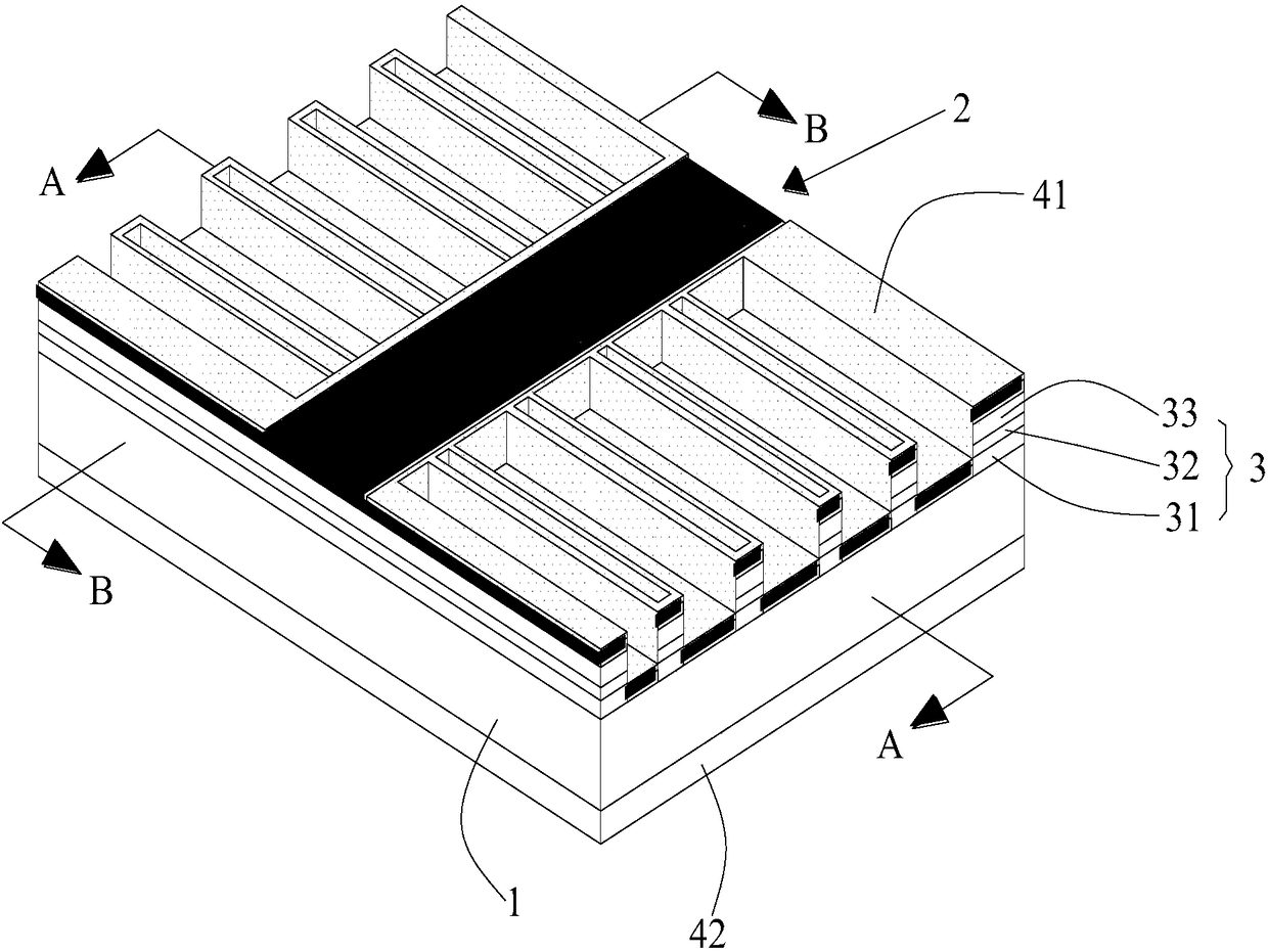
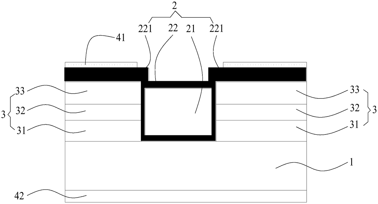
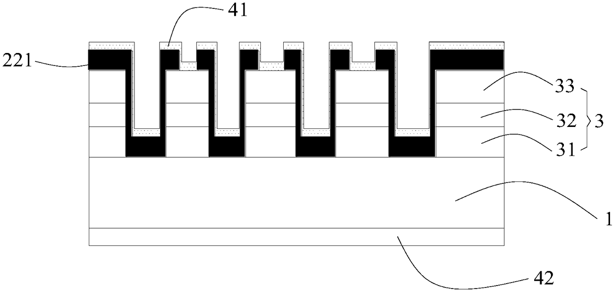
[0045] figure 1 It is a schematic structural diagram of a photonic integrated device according to Embodiment 1 of the present invention; figure 2 yes figure 1 A schematic cross-sectional view of the photonic integrated device along the A-A direction; image 3 yes figure 1 Schematic cross-sectional view of the photonic integrated device along the B-B direction.
[0046] refer to Figure 1-Figure 3 , the present embodiment provides a photonic integrated device, which includes a substrate 1, a two-dimensional material unit 2 disposed on the substrate 1, and semiconductor light emitting units 3 located on both sides of the two-dimensional material unit 2; the semiconductor light emitting unit 3 A positive electrode 41 is provided on the top layer, and a negative electrode 42 is also provided on the substrate 1 .
[0047] The two-dimensional material unit 2 is provided with a light-emitting two-dimensional material 21 whose light-emitting band is longer than that of the semic...
Embodiment 2
[0060] In the description of Embodiment 2, the similarities with Embodiment 1 will not be repeated here, and only the differences with Embodiment 1 will be described. refer to Figure 4 and Figure 5 The difference between embodiment 2 and embodiment 1 is that part of the lower structure layer 31 in the plurality of semiconductor light emitting units 3 is extended and connected as a whole, and at the same time, the extension part 221 covers the part between the plurality of semiconductor light emitting units 3 on the lower structural layer 31.
[0061] In this embodiment, the part of the lower structure layer 31 that is extended and connected as a whole specifically refers to the buffer layer, the lower cladding layer, and a part of the lower waveguide layer adjacent to the lower cladding layer.
Embodiment 3
[0063] In the description of Embodiment 3, the similarities with Embodiment 1 will not be repeated here, and only the differences with Embodiment 1 will be described. refer to Figure 6 and Figure 7 The difference between embodiment 3 and embodiment 1 is that the lower structure layer 31, the active layer 32 and part of the upper structure layer 33 in the plurality of semiconductor light-emitting units 3 are simultaneously extended and connected as a whole, and the extension part 221 covers the plurality of On the part of the upper structure layer 33 between the two semiconductor light emitting units 3; at the same time, an angle not equal to 90° is also formed between the semiconductor light emitting unit 3 and the two-dimensional material unit 2; thus, the semiconductor light emitting unit 3 is specifically superradiant glow tube.
[0064] In this embodiment, the part of the upper structure layer 33 that is extended and connected as a whole specifically refers to the part...
PUM
 Abstract
Description
Claims
Application Information
 - R&D Engineer
- R&D Manager
- IP Professional
- Industry Leading Data Capabilities
- Powerful AI technology
- Patent DNA Extraction
Browse by: Latest US Patents, China's latest patents, Technical Efficacy Thesaurus, Application Domain, Technology Topic, Popular Technical Reports.
© 2024 PatSnap. All rights reserved.Legal|Privacy policy|Modern Slavery Act Transparency Statement|Sitemap|About US| Contact US: help@patsnap.com


