Polycrystalline gallium-doped back passivation solar cell and preparation method thereof
A solar cell and back passivation technology, which is applied in the field of solar cells, can solve the problems of reducing the lifetime of minority carriers, reducing the efficiency of solar cells, reducing the diffusion length of minority carriers, etc., and achieving the effect of light attenuation control
- Summary
- Abstract
- Description
- Claims
- Application Information
AI Technical Summary
Problems solved by technology
Method used
Image
Examples
preparation example Construction
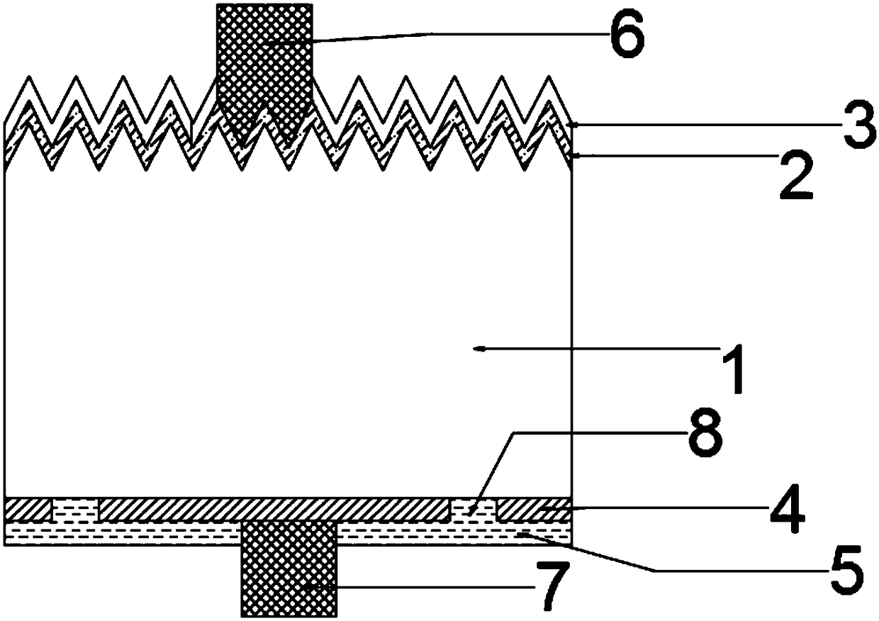
[0043] A method for preparing a solar cell of the present invention comprises the following steps:
[0044] 1) Surface texturing and cleaning the gallium-doped silicon substrate; the surface texturing process is an acid texturing process, or reactive ion etching texturing, or silver ion assisted texturing.
[0045] 2) Prepare the emitter;
[0046] 3) Perform edge insulation treatment; the insulation treatment method is a wet etching method, and the wet etching method includes the use of HNO-containing 3 , HF mixed acidic solution or chemical etching method using alkaline solution containing potassium hydroxide, sodium hydroxide, tetramethylammonium hydroxide, etc.
[0047] 4) Preparation of passivation anti-reflection film on the front side and preparation of passivation film on the back side;
[0048] 5) Perform local film opening on the back passivation film; the local film opening process of the passivation film can use chemical etching slurry to form local contact patter...
Embodiment 1
[0053] The first step is to texture the surface of the polycrystalline gallium-doped silicon wafer; the width of the gallium-doped silicon wafer is 156.75mm, the diameter is 220mm, the silicon wafer does not contain boron, and the concentration of gallium is 2×10 16 atoms / cubic centimeter. For this, the polycrystalline gallium-doped silicon wafer is textured by using HF / HNO3 solution in a chain cleaner to form a pyramid structure on the surface. The temperature of the solution is 7°C, and the duration is 1-5min. And after KOH cleaning, HF pickling, water washing, drying and other steps, the surface metal ions are removed.
[0054] The second step is to prepare the emitter. The preparation of the pn junction is completed in the tubular heating diffusion furnace tube, using N2 to carry the POCl3 source. The diffusion peak temperature was 850°C, and the diffusion time was 110 minutes.
[0055] The third step is to carry out insulation treatment. The insulation treatment is c...
Embodiment 2
[0061] The first step is to texture the surface of the polycrystalline gallium-doped silicon wafer; the gallium-doped silicon wafer has a side-to-side distance of 156 mm and a diameter of 210 mm. The silicon wafer substrate contains boron, and the concentration of boron is 3×10 15 atoms / cm3, containing gallium at a concentration of 3×10 15 atoms / cubic centimeter. For this, the polycrystalline gallium-doped silicon wafer is textured by using HF / HNO3 solution in a chain cleaner to form a pyramid structure on the surface. The temperature of the solution is 7°C, and the duration is 1-5min. And after KOH cleaning, HF pickling, water washing, drying and other steps, the surface metal ions are removed.
[0062] The second step is to prepare the emitter. The preparation of the pn junction is completed in the tubular heating diffusion furnace tube, using N2 to carry the POCl3 source. The diffusion peak temperature is 830°C, and the diffusion time is 90 minutes.
[0063] The third ...
PUM
| Property | Measurement | Unit |
|---|---|---|
| Thickness | aaaaa | aaaaa |
| Thickness | aaaaa | aaaaa |
| Thickness | aaaaa | aaaaa |
Abstract
Description
Claims
Application Information
 - R&D Engineer
- R&D Manager
- IP Professional
- Industry Leading Data Capabilities
- Powerful AI technology
- Patent DNA Extraction
Browse by: Latest US Patents, China's latest patents, Technical Efficacy Thesaurus, Application Domain, Technology Topic, Popular Technical Reports.
© 2024 PatSnap. All rights reserved.Legal|Privacy policy|Modern Slavery Act Transparency Statement|Sitemap|About US| Contact US: help@patsnap.com


