
Preparation method and application of water-soluble SnO2 inorganic semiconductor nanomaterial

A technology of inorganic semiconductors and nanomaterials, applied in the direction of organic semiconductor devices, semiconductor/solid-state device manufacturing, semiconductor devices, etc., can solve the problems of no further exploration of SnO dispersion ability, no further exploration of dispersion effect, unfavorable practical applications, etc., to achieve Good practical application value, good dispersion effect, low cost effect

Inactive Publication Date: 2018-06-15
NINGBO UNIVERSITY OF TECHNOLOGY
View PDF4 Cites 9 Cited by
  • Summary
  • Abstract
  • Description
  • Claims
  • Application Information

AI Technical Summary

Problems solved by technology

However, it did not go further to explore the SnO 2 Dispersion ability in different solvents, which is an indispensable issue for the direct use of this nanomaterial to prepare thin films
Therefore, SnO 2 The problem of dispersion of nanomaterials leads to the most widely used SnO 2 The film-making method is still based on the precursor heat treatment method, although compared with TiO 2 The required temperature is greatly reduced, but it is still not conducive to large-scale practical applications
Alex K.-Y.Jen et al. reported that they used isopropanol to disperse SnO 2 nanoparticles, and can get flatter SnO 2 thin films, but it did not further explore the SnO it synthesized 2 Dispersion effect of nanoparticles in other solvents
However, the most widely used SnO 2 The film-making method is still based on the precursor heat treatment method, although compared with TiO 2 The required temperature is greatly reduced, but it is still not conducive to large-scale practical applications

Method used


Image

  • Preparation method and application of water-soluble SnO2 inorganic semiconductor nanomaterial
  • Preparation method and application of water-soluble SnO2 inorganic semiconductor nanomaterial
  • Preparation method and application of water-soluble SnO2 inorganic semiconductor nanomaterial

Examples


Embodiment 1

[0041] Embodiment 1, water-soluble SnO 2 Preparation of Inorganic Semiconductor Nanomaterials

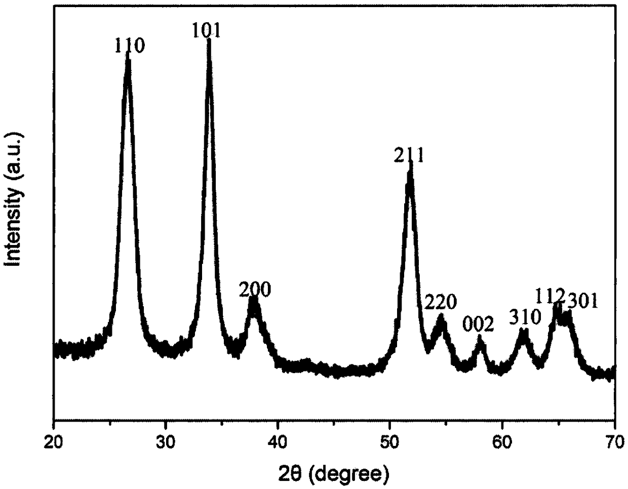
[0042] Weigh 350mg of SnCl 4 ·5H2 O was dissolved in 6 mL of a mixed solvent of water and ethanol, the volume ratio of the mixed solvent of water and ethanol was 1:3, and stirred at room temperature until a clear solution was formed, and then 6 mL of 9% tetramethanone was added Ammonium hydroxide aqueous solution will produce white flocs in the solution instantly, stir vigorously until a clear and transparent solution is formed, and then transfer the clear and transparent solution to a polytetrafluoroethylene-lined autoclave, at 195 ° C Under the conditions of hydrothermal reaction for 12h. After natural cooling to room temperature, add 35mL of acetone to the clear solution to precipitate the product, remove the supernatant, disperse the precipitate in 10mL of ultrapure water to obtain a clear and transparent solution again, and then use 35mL of acetone to precipitate the product ...

Embodiment 2

[0045] Embodiment 2, described SnO 2 Preparation of Dispersion System of Inorganic Semiconductor Nanomaterials in Water Phase and Trifluoroethanol Phase

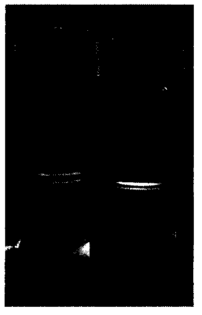
[0046] Weigh 100mg of the product obtained in Example 1, measure into 2mL of ultrapure water, and shake slightly to obtain 50mg / mL of aqueous SnO 2 Dispersion system; Weigh 20mg of the product obtained in Example 1, measure into 2mL of trifluoroethanol, ultrasonic 1h and stir for 12h to obtain 10mg / mL of trifluoroethanol phase SnO 2 decentralized system.

Embodiment 3

[0047] Embodiment 3, described SnO 2 Preparation of thin films of inorganic semiconductor nanomaterials

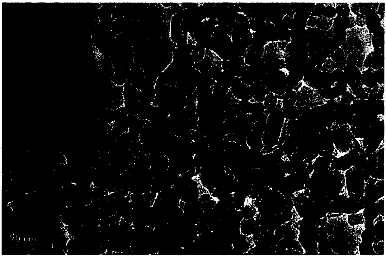
[0048] Prepare the aqueous phase SnO of the present invention of 30mg / mL by the method for embodiment 2 2 Dispersion system, SnO was prepared by spin coating on ITO substrate 2 Thin film; the trifluoroethanol phase SnO of the present invention prepared 10mg / mL by the method of embodiment 2 2 Dispersion system, SnO was prepared by spin-coating method on perovskite film 2 film. With the SnO prepared on ITO in embodiment 3 2 Surface morphology of thin films and SnO prepared by spin-coating method on perovskite thin films 2 Scanning electron microscopy (SEM) experiments were performed on the surface morphology of the films, and the results were as follows: Figure 4 shown.


PUM

PropertyMeasurementUnit
crystal sizeaaaaaaaaaa
sizeaaaaaaaaaa
particle sizeaaaaaaaaaa

Abstract

The invention discloses a preparation method and application of a water-soluble SnO2 inorganic semiconductor nanomaterial. The preparation method comprises the following steps: dissolving SnCl4.5H2O into a mixed solvent of water and ethanol, and adding a 8-10% tetramethylammonium hydroxide water solution; then, carrying out a hydro-thermal synthesis reaction; and carrying out acetone precipitationto obtain the water-soluble SnO2 inorganic semiconductor nanomaterial. The water-soluble SnO2 inorganic semiconductor nanomaterial disclosed by the invention not only has excellent dispersibility inwater, but also has relatively good dispersibility in trifluoroethanol, so that the water-soluble SnO2 inorganic semiconductor nanomaterial can be used for coating an ITO or perovskite film by using aspin-coating method to obtain an SnO2 film; and the preparation method is safe, simple, low in cost and environment-friendly.

Description

technical field [0001] The invention relates to a water-soluble SnO 2 Preparation methods and applications of inorganic semiconductor nanomaterials. Background technique [0002] Inorganic semiconductor nanomaterials have shown unique advantages in the field of photovoltaics, because compared with organic semiconductor materials, they have the characteristics of simple preparation, low cost, and air stability, which are conducive to large-scale commercial applications. Today, TiO 2 Perovskite solar cells are still the most widely used inorganic semiconductor materials. However, conventionally used TiO 2 The film-making process requires a heat treatment temperature exceeding 450 °C, which limits the possibility of its large-scale commercial application, and is also not conducive to the manufacture of foldable and wearable perovskite solar cells. [0003] Compared to TiO 2 , SnO 2 Has many very superior properties. Its energy band gap exceeds 3.6eV, and it has a higher ...

Claims


Application Information

Patent Timeline
Patent Type & Authority Applications(China)
IPC IPC(8): C01G19/02B82Y30/00C03C17/34H01L51/42H01L51/46H01L51/48B05D1/00B05D7/24
CPCB82Y30/00C01G19/02C03C17/3417B05D1/005B05D7/24C01P2004/04C01P2002/72C03C2218/116H10K30/15H10K2102/00Y02E10/549
Inventor 肖勋文沈梁钧王乐佳
Owner NINGBO UNIVERSITY OF TECHNOLOGY
Learn More