InAs/GaSb superlattice infrared detector and manufacturing method thereof

A technology of infrared detectors and manufacturing methods, applied in the direction of semiconductor devices, final product manufacturing, sustainable manufacturing/processing, etc., can solve problems such as environmental pollution, cost waste, etc., to avoid external stress, improve quality, and make the production process efficient and environmentally friendly Effect

Active Publication Date: 2018-06-08
WUHAN GAOXIN TECH
View PDF8 Cites 6 Cited by
  • Summary
  • Abstract
  • Description
  • Claims
  • Application Information

AI Technical Summary

Problems solved by technology

And the substrate obtained by this method can be reused after polishing and cleaning, which makes the manufacturing process of the entire InAs / GaSb superlattice infrared detector more efficient and environmentally friendly, thus solving the problem of the environment in the removal process of the infrared detector substrate in the prior art. Problems of pollution and cost waste

Method used


Image

  • InAs/GaSb superlattice infrared detector and manufacturing method thereof
  • InAs/GaSb superlattice infrared detector and manufacturing method thereof
  • InAs/GaSb superlattice infrared detector and manufacturing method thereof

Examples


Embodiment Construction

[0044] In order to make the object, technical solution and advantages of the present invention clearer, the present invention will be further described in detail below in conjunction with the accompanying drawings and embodiments. It should be understood that the specific embodiments described here are only used to explain the present invention, not to limit the present invention. In addition, the technical features involved in the various embodiments of the present invention described below can be combined with each other as long as they do not constitute a conflict with each other.

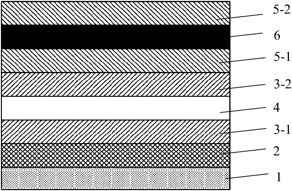
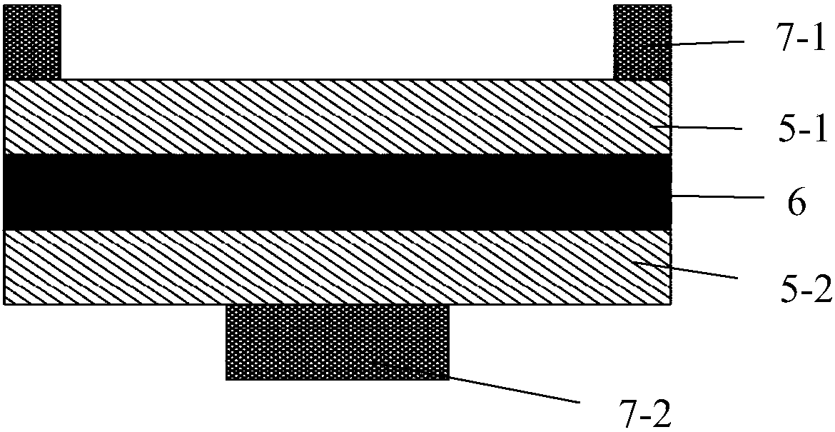
[0045] Such as figure 1 as shown, figure 1 It is a schematic diagram of the structure of an epitaxial wafer of an InAs / GaSb superlattice infrared detector of the present invention, which includes a substrate 1, a buffer layer 2, a first stop layer 3-1, a sacrificial layer 4, and a second stop layer 3 from bottom to top. -2. The first contact layer 5-1, the superlattice structure 6, and the sec...


PUM

PropertyMeasurementUnit
Thicknessaaaaaaaaaa

Abstract

The invention discloses an InAs / GaSb superlattice infrared detector and a manufacturing method thereof. In the prior art, during the epitaxial growth of several hundreds of cycles of InAs / GaSb superlattice materials, lattice mismatching exists between the InAs and GaSb; and lots of growth defects are formed in the InAs / GaSb superlattice materials because of the accumulated stresses. The inventionprovides a two-step Sb infiltration method. An InAs layer grows and then a Sb layer is deposited to form a Sb-rich surface; In is deposited and then a Sb layer is deposited, so that the In and the Sbmakes reaction fully to form a high-quality InSb interface layer. Therefore, the stress between the InAs and GaSb is balanced and eliminated and thus the quality of the InAs / GaSb superlattice materialis improved. Meanwhile, because of introduction of the AlAsSb sacrificial layer between the InAs / GaSb superlattice structure and the GaSb substrate, the non-destructive stripping of the substrate isrealized.

Description

technical field [0001] The invention belongs to the technical field of semiconductor optoelectronic devices, and more specifically relates to an InAs / GaSb superlattice infrared detector and a preparation method thereof. Background technique [0002] Currently, the high-performance infrared detectors on the market are mainly mercury cadmium telluride (HgCdTe) infrared detectors. Hg 1- x Cd x Te is a continuous solid solution of binary compounds CdTe and HgTe with a bandgap E g Dependent on operating temperature and component x value. By continuously changing its forbidden band width (from 0 to 1.6eV), almost all response bands covering important infrared atmospheric windows can be obtained. HgCdTe infrared detector has many advantages such as low noise, high detection rate, high electron mobility, long carrier lifetime, intrinsic transition, large absorption coefficient and high quantum efficiency. With the rapid development of device technology and readout circuits, th...

Claims


Application Information

Patent Timeline
IPC IPC(8): H01L31/0304H01L31/0352H01L31/18
CPCH01L31/03042H01L31/035236H01L31/1844Y02P70/50
Inventor 杨晓杰刘永峰张传杰谭必松周文洪黄立
Owner WUHAN GAOXIN TECH
Why Eureka
Try Eureka