Multi-channel microfluidic chip device for vacuum negative pressure sample injection, preparation method and application thereof
A microfluidic chip, vacuum negative pressure technology, applied in chemical instruments and methods, laboratory containers, laboratory utensils, etc. To achieve the effect of high-throughput accurate quantitative sensing, less sample consumption, and accurate quantitative sensing
- Summary
- Abstract
- Description
- Claims
- Application Information
AI Technical Summary
Problems solved by technology
Method used
Image
Examples
Embodiment 1
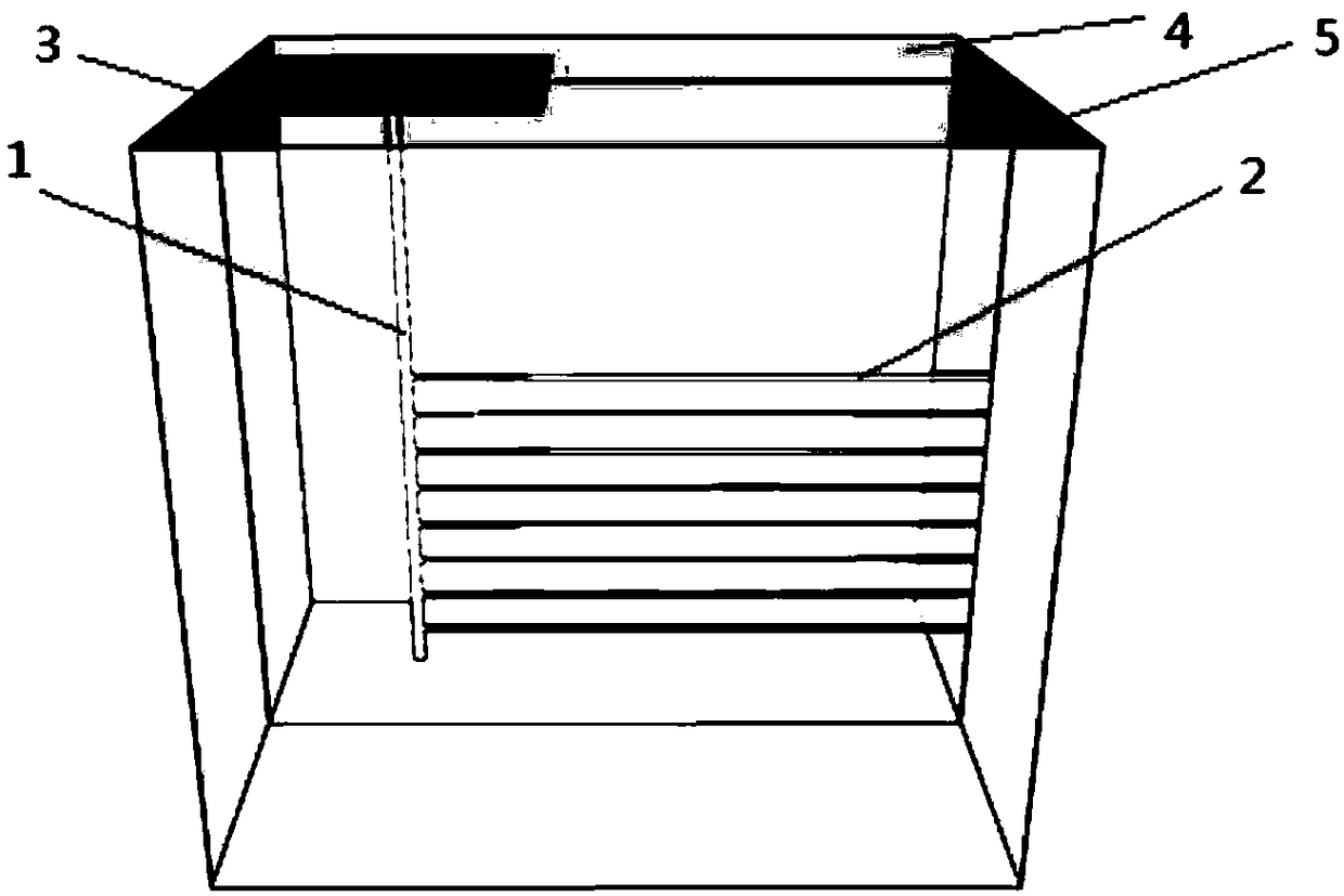
[0052] In this embodiment, the multi-channel microfluidic chip detection device for vacuum negative pressure sampling and blood filtration consists of two parts: a microfluidic chip and a microporous filter membrane. Such as figure 1 As shown, the microfluidic chip is a polydimethylsiloxane (PDMS) microfluidic chip, which is formed by bonding a PDMS thin layer engraved with a microchannel structure and a PDMS thin layer without a microchannel.
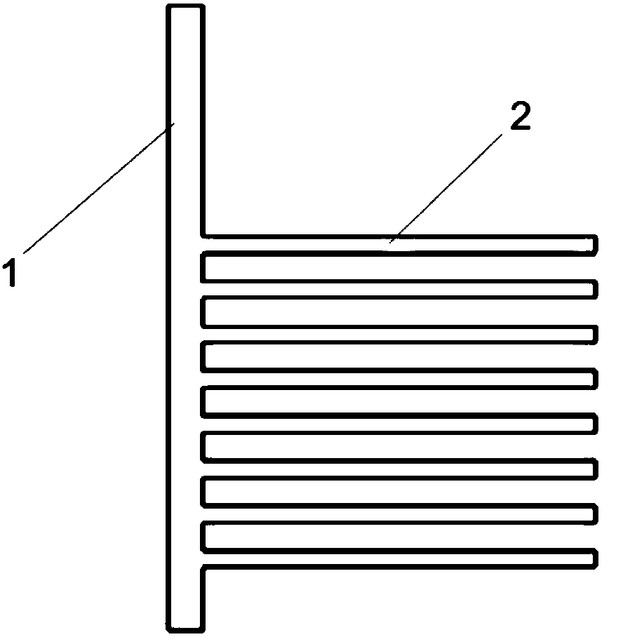
[0053] The microchannel structure in the PDMS thin layer is a main channel connected vertically to eight parallel sample loading channels, and the structure of the entire microchannel is similar to a comb shape, as shown in figure 2 shown.
[0054] In this embodiment, the eight sample loading channels are located on the same side of the main channel, and the channel width and distance between channels are set to be the same.
[0055] The specific dimensions or data used in the description of the microchannel structure in this embodi...
Embodiment 2
[0058] The preparation method of the multi-channel microfluidic chip device for vacuum negative pressure sampling in the present invention comprises the following steps:
[0059] (1) Fabrication of PDMS microfluidic chip, the process can be found in Figure 4 , the specific production process can be divided into the following steps:
[0060] (1-1) Mask design and production: design the mask pattern of the microfluidic chip, and print the mask pattern on the film through a printer (resolution greater than 20000dpi) to obtain a film mask.
[0061] (1-2) Substrate cleaning and uniform glue: After the substrate is strictly cleaned with acetone, Piranha solution and ultrapure water and dried at high temperature (150℃×1h), add an appropriate amount of SU-8 photoresist dropwise in the center of the substrate (about 1ml / inch 2 ), put it on the turntable of the homogenizer, and adopt the program of 600rpm×18s, 2100rpm×60s (increase the speed at 100rpm / min) to homogenize the glue. Th...
Embodiment 3
[0078] A multi-channel microfluidic chip detection device for vacuum negative pressure sampling and blood filtration. The microfluidic chip is formed by bonding a polydimethylsiloxane (PDMS) thin layer carved with a microchannel and a PDMS thin layer without a microchannel. Make a crosscut on the two bonded PDMS to expose the main channel of the microchannel, apply a layer of glue around the exposed main channel opening at a certain distance, and stick a small piece of BTS film on the glue to make the main channel opening is sealed, thus forming the final chip device.
[0079] The microchannel structure is connected by an inlet channel and eight outlet channels, and its structural characteristics are as follows: the solution inlet channel (hereinafter referred to as the main channel) is a straight channel, which is connected with eight solution outlet channels (hereinafter referred to as the sample loading channel). The eight sample loading channels are arranged in parallel, ...
PUM
 Abstract
Description
Claims
Application Information
 - R&D
- Intellectual Property
- Life Sciences
- Materials
- Tech Scout
- Unparalleled Data Quality
- Higher Quality Content
- 60% Fewer Hallucinations
Browse by: Latest US Patents, China's latest patents, Technical Efficacy Thesaurus, Application Domain, Technology Topic, Popular Technical Reports.
© 2025 PatSnap. All rights reserved.Legal|Privacy policy|Modern Slavery Act Transparency Statement|Sitemap|About US| Contact US: help@patsnap.com


