Vertical double diffusion field effect transistor and manufacture method thereof

A technology of field effect transistors and vertical double diffusion, which is applied in the direction of semiconductor devices, electrical components, circuits, etc., can solve problems affecting device performance and achieve the effects of improving device performance, reducing parasitic capacitance, and reducing local resistivity

Inactive Publication Date: 2018-05-22
SHENZHEN JINGTE INTELLIGENT MFG TECH CO LTD
View PDF3 Cites 0 Cited by
  • Summary
  • Abstract
  • Description
  • Claims
  • Application Information

AI Technical Summary

Problems solved by technology

However, N-type implantation is a full-chip implantation, and non-JFET regions will also be implanted, which will affect device performance.

Method used


Image

  • Vertical double diffusion field effect transistor and manufacture method thereof
  • Vertical double diffusion field effect transistor and manufacture method thereof
  • Vertical double diffusion field effect transistor and manufacture method thereof

Examples


Embodiment Construction

[0028] The following will clearly and completely describe the technical solutions in the embodiments of the present invention. Obviously, the described embodiments are only some of the embodiments of the present invention, rather than all the embodiments. Based on the embodiments of the present invention, all other embodiments obtained by persons of ordinary skill in the art without making creative efforts belong to the protection scope of the present invention.

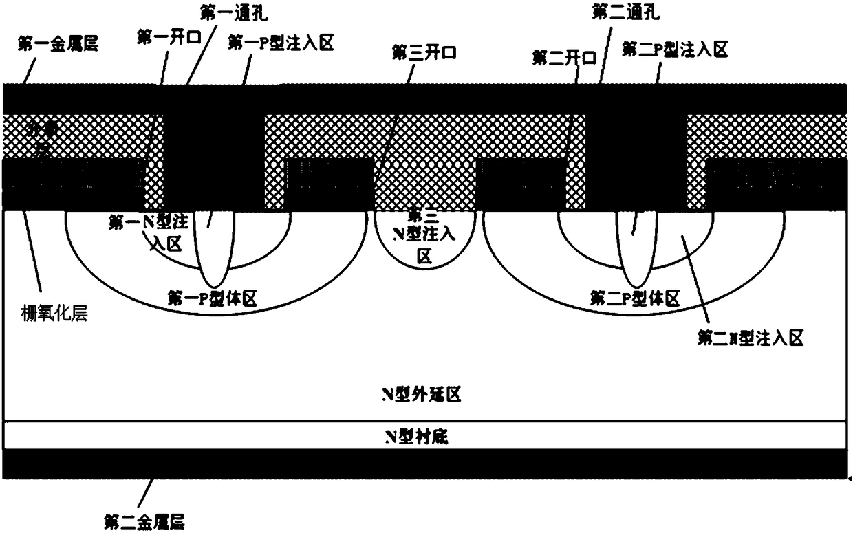
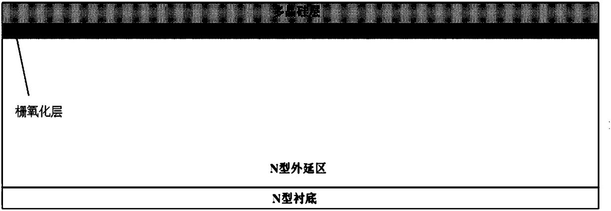
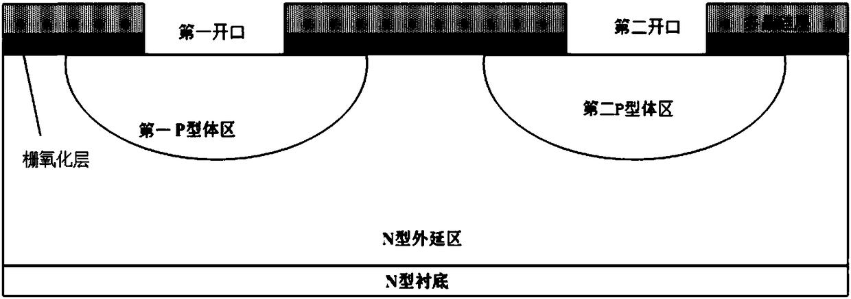
[0029] see figure 1 , figure 1It is a schematic diagram of the cross-sectional structure of the vertical double-diffused field effect transistor provided by the present invention. The vertical double diffused field effect transistor includes an N-type substrate, an N-type epitaxial region formed on the N-type substrate, a first P-type body region and a second P-type body region formed on the surface of the N-type epitaxial region. body region, a first N-type implant region located on the surface of the first P-type...


PUM


Abstract

A vertical double diffusion field effect transistor includes an N-type substrate, an N-type epitaxial region; a first P-type body region and a second P-type body region formed on the surface of the N-type epitaxial region; a first N-type injection region disposed on the surface of the first P-type body region; a second N-type injection region disposed on the surface of the second P-type body region; a third N-type injection region disposed on the surface of the N-type epitaxial region; a first P-type injection region penetrating through the first N-type injection region and extending to the first P-type body region; a second P-type injection region penetrating through the second N-type injection region and extending to the second P-type body region; gate oxide layers and polycrystalline silicon layers formed on the N-type epitaxial region, the first and the second P-type body regions, the first and the second N-type injection regions; medium layers formed on the polycrystalline siliconlayers, the first, the second and the third N-type injection regions; a first through hole penetrating through the medium layers and corresponding to the first N-type injection region and the first P-type injection region; and a second through hole penetrating through the medium layer and corresponding to the second N-type injection region and the second P-type injection region.

Description

【Technical field】 [0001] The invention relates to the technical field of semiconductor chip fabrication, in particular to a vertical double diffused field effect transistor (VDMOS) and a fabrication method thereof. 【Background technique】 [0002] The drain and source poles of the vertical double diffused field effect transistor (VDMOS) are respectively on both sides of the device, so that the current flows vertically inside the device, increasing the current density, improving the rated current, and the on-resistance per unit area is also small, which is a A very versatile power device. The most important performance parameter of a vertical double diffused field effect transistor (VDMOS) is the operating loss, which can be divided into three parts: conduction loss, cut-off loss and switching loss. The conduction loss is determined by the conduction resistance, the cut-off loss is affected by the reverse leakage current, and the switching loss refers to the loss caused by th...

Claims


Application Information

Patent Timeline
Patent Type & Authority Applications(China)
IPC IPC(8): H01L29/10H01L29/66H01L29/78
CPCH01L29/7802H01L29/10H01L29/66712
Inventor 不公告发明人
Owner SHENZHEN JINGTE INTELLIGENT MFG TECH CO LTD
Why Eureka
Try Eureka