Physical vapor deposition device and method

A physical vapor deposition, vapor deposition technology, applied in ion implantation plating, metal material coating process, coating, etc., to achieve the effect of improving product yield, reducing temperature difference, and reducing temperature difference

Inactive Publication Date: 2018-05-11
SHANGHAI HUALI MICROELECTRONICS CORP
View PDF5 Cites 2 Cited by
  • Summary
  • Abstract
  • Description
  • Claims
  • Application Information

AI Technical Summary

Problems solved by technology

[0004] The technical problem to be solved by the present invention is to provide a physical vapor deposition equipment, which can control and reduce the temperature difference in each area of ​​the wafer during the operation process, thereby eliminating the metal damage caused by the temperature difference during the wafer operation process. Lattice defects

Method used


Image

  • Physical vapor deposition device and method
  • Physical vapor deposition device and method
  • Physical vapor deposition device and method

Examples


Embodiment Construction

[0037] The technical solution of the embodiment of the present invention is designed for the technical problem to be solved after an in-depth analysis of the technical problem proposed by the present invention, so before introducing the technical solution of the embodiment of the present invention in detail, first introduce the technical problem of the present invention. and its analysis process:

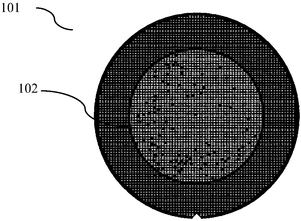
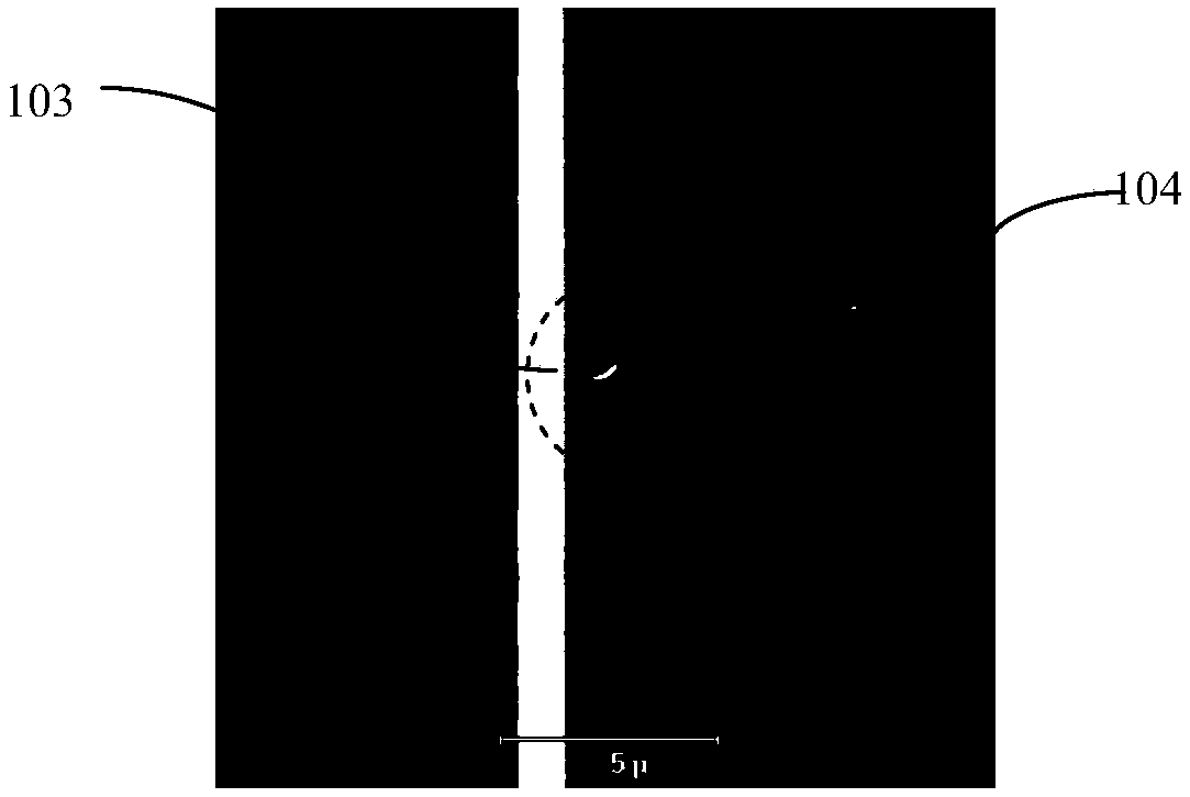
[0038] With the development of integrated circuit technology and the increase of wafer size, semiconductor production puts forward higher requirements for temperature uniformity in the process of thin film deposition. At present, the physical vapor deposition thickness of aluminum in the back-end of the semiconductor is relatively large, and the operating temperature is relatively high. During the operation process, there is a certain gradient in the temperature of the entire wafer. Due to the sensitivity of the aluminum deposition layer to temperature differences, hilly defects are...


PUM


Abstract

The invention discloses a physical vapor deposition device. The physical vapor deposition device is characterized in that a vapor deposition process chamber comprises a wafer base, wherein a cooling water channel for controlling wafer cooling is arranged in the wafer base and divided into a plurality of independent circulating areas; each independent circulating area is used for correspondingly cooling the rear surface, in the corresponding area, of the wafer; the cooling rate of each independent circulating area is independently adjusted, so that the cooling rate of each area is kept consistent when the wafer is in the working process, and the temperature difference between the areas can be reduced when the wafer is in the working process, and moreover, the temperature difference is reduced to reach the level that metal lattice defects are not caused. The invention also discloses a physical vapor deposition method. With the adoption of the device and the method, the temperature difference among the areas can be controlled when the wafer is in the working process, and the temperature difference is reduced, so that the metal lattice defects caused by the temperature difference occurring in the working process of the wafer can be removed, and as a result, the product yield is increased.

Description

technical field [0001] The invention relates to the manufacture of semiconductor integrated circuits, in particular to a physical vapor deposition (PVD) device. The invention also relates to a physical vapor deposition method. Background technique [0002] With the development of integrated circuit technology and the increase of wafer size, semiconductor production puts forward higher requirements for temperature uniformity in the process of thin film deposition. [0003] At present, the physical vapor deposition thickness of aluminum in the back-end of the semiconductor is relatively large, and the operating temperature is relatively high. During the operation process, there is a certain gradient in the temperature of the entire wafer. Due to the sensitivity of the aluminum deposition layer to temperature differences, hilly defects are prone to occur when the temperature is low, and whisker defects are prone to occur when the temperature is high. Therefore, non-uniform gro...

Claims


Application Information

Patent Timeline
IPC IPC(8): C23C14/54C23C14/50
CPCC23C14/541C23C14/50
Inventor 瞿燕龙吟倪棋梁王恺
Owner SHANGHAI HUALI MICROELECTRONICS CORP
Why Eureka
Try Eureka