Perovskite solar cell, double-layer metal electrode and preparation method thereof
A technology of solar cells and double-layer metals, applied in circuits, electrical components, electrical solid devices, etc., can solve the problem of low stability of metal electrodes and achieve the effect of improving stability
- Summary
- Abstract
- Description
- Claims
- Application Information
AI Technical Summary
Problems solved by technology
Method used
Image
Examples
Embodiment 1
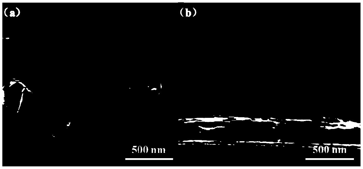
[0028] Such as figure 2 As shown, it is the interface SEM photo and EDS energy spectrum analysis diagram of the perovskite solar cell based on Bi / Ag and Bi / Mo double-layer metal electrodes, wherein, figure 2 a is a Bi / Ag double-layer metal electrode, that is, the first metal film layer is a 20nm thick Bi metal layer, and the second metal film layer is a 150nm thick Ag metal layer; figure 2 b is a Bi / Mo double-layer metal electrode, that is, the first metal thin film layer is a Bi metal layer with a thickness of 20 nm, and the second metal thin film layer is a Mo metal layer with a thickness of 500 nm.
Embodiment 2
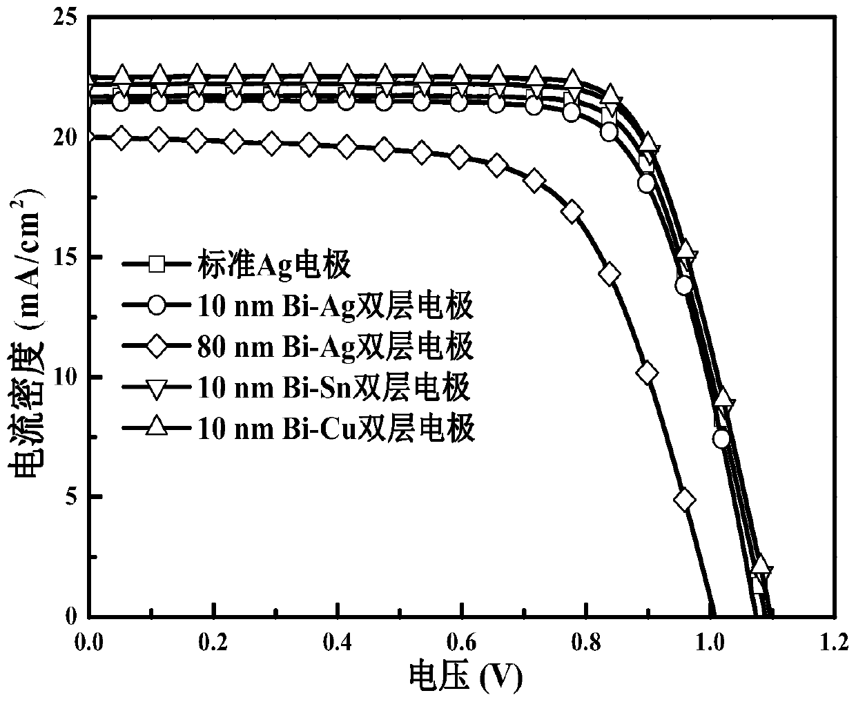
[0030] Five sets of perovskite solar cells were prepared under the same conditions. The inability of the five sets of perovskite solar cells is: the first set of single-layer Ag metal electrodes; the second set of double-layer metal electrodes, and the first layer is Bi Metal layer, the second layer is Ag metal layer, the thickness of Bi metal layer is 10nm; the third group is double-layer metal electrode, and the first layer is Bi metal layer, the second layer is Ag metal layer, and the thickness of Bi metal layer is 80nm ; The fourth group is a double-layer metal electrode, and the first layer is a Bi-Sn alloy metal layer, the second layer is an Ag metal layer, and the thickness of the Bi-Sn alloy metal layer is 10nm; the fifth group is a double-layer metal electrode, and The first layer is a Bi-Cu alloy metal layer, the second layer is an Ag metal layer, and the thickness of the Bi-Cu alloy metal layer is 10nm.
[0031] Select an area of 1cm 2 The above five groups of pe...
Embodiment 3
[0033]Taking four groups of halide perovskites (CH 3 NH 3 PB 3 ) film at 35°C and 70% humidity, choose different covering methods, and measure the decomposition products (PbI 2 ), such as image 3 Shown, from bottom to top are the XRD patterns of the first to eighth. Among them, the first one is: the first group of halide perovskite films were placed under the standard metal Ag electrode (which is equivalent to not covering Bi) for two days; the second one was: the second group of halide perovskite films were exposed to Bi The film is covered for two days, which is equivalent to that the first metal film layer is a Bi metal film layer, and the second metal film layer is an Ag metal film layer; Two days, it is equivalent to the first metal film layer is a Bi-Sn alloy film, the second metal film layer is an Ag metal film layer; the fourth is: the fourth group of halide perovskite films covered by Bi-Cu metal film Two days, it is equivalent to that the first metal film layer...
PUM
| Property | Measurement | Unit |
|---|---|---|
| thickness | aaaaa | aaaaa |
| thickness | aaaaa | aaaaa |
| thickness | aaaaa | aaaaa |
Abstract
Description
Claims
Application Information
 - R&D
- Intellectual Property
- Life Sciences
- Materials
- Tech Scout
- Unparalleled Data Quality
- Higher Quality Content
- 60% Fewer Hallucinations
Browse by: Latest US Patents, China's latest patents, Technical Efficacy Thesaurus, Application Domain, Technology Topic, Popular Technical Reports.
© 2025 PatSnap. All rights reserved.Legal|Privacy policy|Modern Slavery Act Transparency Statement|Sitemap|About US| Contact US: help@patsnap.com


