
A 3d NAND channel hole forming method based on oxide-polysilicon film stack

A technology of polysilicon thin film and oxide film layer, which is applied to semiconductor devices, electrical components, circuits, etc., can solve the problem of not being able to etch channel holes at one time, and achieve the effect of avoiding curved arcs and defects

Active Publication Date: 2020-05-12
YANGTZE MEMORY TECH CO LTD
View PDF6 Cites 0 Cited by
  • Summary
  • Abstract
  • Description
  • Claims
  • Application Information

AI Technical Summary

Problems solved by technology

[0009] As mentioned before, due to the use of polysilicon film, in addition to the serious curved arc of the channel hole, polysilicon etching will produce serious polymer, which will cause serious defects, when the film stack reaches 64 layers or more, It will not be possible to etch the channel hole in one pass

Method used


Image

  • A 3d NAND channel hole forming method based on oxide-polysilicon film stack
  • A 3d NAND channel hole forming method based on oxide-polysilicon film stack
  • A 3d NAND channel hole forming method based on oxide-polysilicon film stack

Examples


Embodiment Construction

[0034] Exemplary embodiments of the present disclosure will be described in more detail below with reference to the accompanying drawings. Although exemplary embodiments of the present disclosure are shown in the drawings, it should be understood that the present disclosure may be embodied in various forms and should not be limited by the embodiments set forth herein. Rather, these embodiments are provided for more thorough understanding of the present disclosure and to fully convey the scope of the present disclosure to those skilled in the art.

[0035] In the interest of clarity, not all features of an actual implementation are described. In the following description, well-known functions and constructions are not described in detail since they would obscure the invention with unnecessary detail. It should be appreciated that in the development of any actual embodiment, numerous implementation details must be worked out to achieve the developer's specific goals, such as ch...


PUM


Abstract

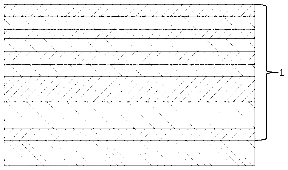
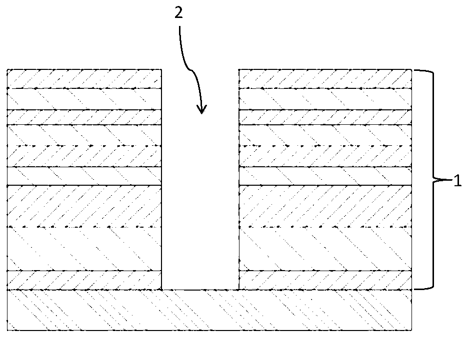
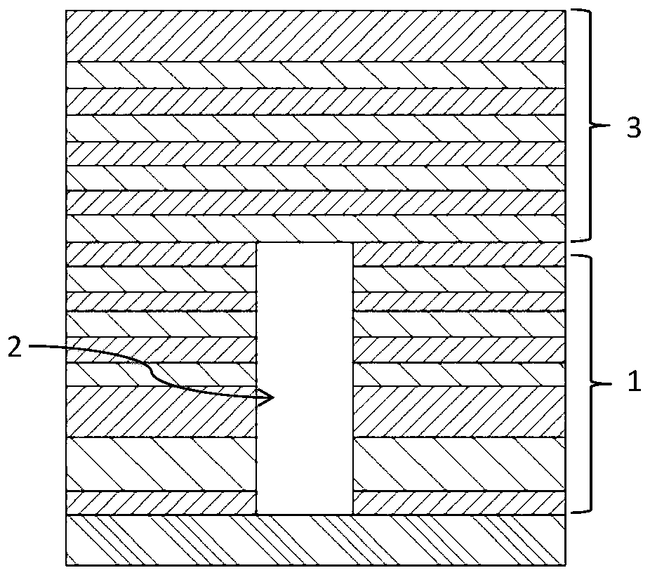
The invention provides a method for forming a 3D NAND channel hole based on oxide-polysilicon film stacking, the method comprising forming a single oxide film layer on a substrate, and the thickness of the film layer is equal to the expected oxide-polysilicon film The thickness of the number of stacked layers; etching on the single oxide film layer to form a channel hole and depositing a structural layer inside the channel hole; depositing silicon nitride in the middle of the internal structure layer; wet etching to remove the channel A single oxide film layer around the hole; and then alternately depositing oxide and polysilicon on the substrate to form a thin film stack structure around the channel hole. The present invention is easier to etch channel holes on a single oxide film layer; can avoid curved arcs of channel holes caused by polysilicon, and avoid defects caused by heavy polymers produced by polysilicon etching. When the number of film stacked layers reaches 64 layers or more, this method can also realize channel hole formation at one time.

Description

technical field [0001] The invention relates to the field of semiconductor manufacturing, in particular to a method for forming channel holes in a 3D NAND flash memory structure. Background technique [0002] With the development of planar flash memory, the production process of semiconductors has made great progress. However, in recent years, the development of planar flash memory has encountered various challenges: physical limits, existing development technology limits, and storage electron density limits. In this context, in order to solve the difficulties encountered in planar flash memory and to seek lower production costs per unit storage unit, various three-dimensional (3D) flash memory structures have emerged, such as 3D NOR (3D or not) flash memory and 3D NAND (3D NAND) flash memory. At present, in the development process of 3D NAND, as the number of stacked layers increases, higher requirements are put forward for the preparation processes such as etching and de...

Claims


Application Information

Patent Timeline
Patent Type & Authority Patents(China)
IPC IPC(8): H01L27/11578
CPCH10B43/20
Inventor 方振黄竹青黄海辉闫伟明戴绍龙王猛金永群
Owner YANGTZE MEMORY TECH CO LTD
Learn More