Manufacturing method of 3D NAND

A manufacturing method and technology of substrate structure, applied in electrical components, electric solid state devices, circuits, etc., can solve problems such as yield reduction, device reliability and frequency reduction, and wafer scrapping.

Active Publication Date: 2018-05-04
YANGTZE MEMORY TECH CO LTD
View PDF5 Cites 3 Cited by
  • Summary
  • Abstract
  • Description
  • Claims
  • Application Information

AI Technical Summary

Problems solved by technology

The problem of arc discharge will directly lead to the scrapping of the wafer, resulting in a decrease in yield, and the problem of edge peeling will also lead to a decrease in the reliability and frequency of the device

Method used


Image

  • Manufacturing method of 3D NAND
  • Manufacturing method of 3D NAND
  • Manufacturing method of 3D NAND

Examples


Embodiment Construction

[0025] Exemplary embodiments of the present disclosure will be described in more detail below with reference to the accompanying drawings. Although exemplary embodiments of the present disclosure are shown in the drawings, it should be understood that the present disclosure may be embodied in various forms and should not be limited by the embodiments set forth herein. Rather, these embodiments are provided for more thorough understanding of the present disclosure and to fully convey the scope of the present disclosure to those skilled in the art.

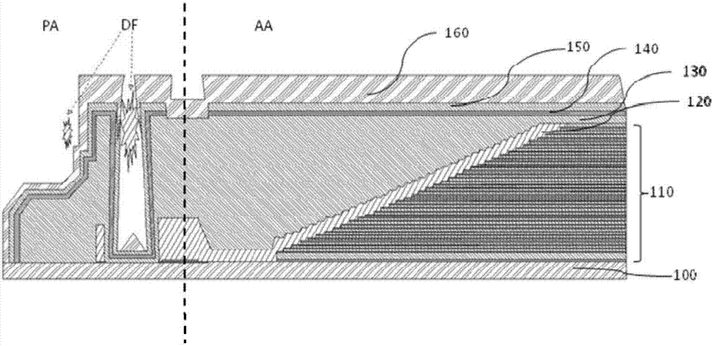
[0026] Figure 3(a)-3(g) A method of forming 3D NAND according to one embodiment of the invention is shown.

[0027] First, a substrate structure is provided, which has a substrate 300 , a stepped structure 310 formed with an ON stack formed on the substrate 300 , a high density plasma (HDP) deposited layer 320 and a TEOS layer 330 covering the stepped structure 310 .

[0028] As shown in FIG. 3( a ), after the steps are formed, c...


PUM


Abstract

The invention provides a manufacturing method of a 3D NAND. The manufacturing method comprises the following steps of performing depositing to form a barrier layer (320) and a filling layer (330) before performing polysilicon channel etching; performing coating of a negative photoresist layer; adopting a negative photoresist WEE (wafer edge exposure) process, and remaining the negative photoresiston the edge of the wafer; etching and removing the filling layer exposed from the negative photoresist, wherein the barrier layer and the filling layer are high in etching selection ratio, so that the barrier layer is used as an etching barrier layer; removing the residual filling layer (331) by adopting a CMP process, wherein the barrier layer (320) is used as a CMP barrier layer; and removing the barrier layer (320), wherein preferably, the barrier layer is a PECVD deposited SiN layer, and the filling layer is an HDP deposited silicon oxide layer. By virtue of the process, electric arc andstripping defects on the edge of the wafer in the 3D NAND process can be avoided, and the rate of finished product of the wafer is improved.

Description

technical field [0001] The invention relates to a 3D NAND manufacturing method, in particular to a novel process for avoiding wafer edge discharge and peeling problems. Background technique [0002] As a technology of stacking data units, 3D NAND flash memory has increased storage capacity and reduced the storage cost of each data bit, and has become a mainstream storage technology. Vertically stacked 3D NAND flash memory is a common device stacking method. [0003] A traditional 3D NAND flash memory core includes a substrate 100 including a central area (AA) and a peripheral area (PA), and its manufacturing method includes: forming a peripheral gate structure in the peripheral area; forming an ON stack layer in the central area, by photolithography / lithography The step structure 110 is formed by etching, and the trim / Etch method can be used for the photolithography; a high-density plasma deposition (HDPdeposition) layer 120 and a TEOS deposition layer 130 are performed on t...

Claims


Application Information

Patent Timeline
IPC IPC(8): H01L27/1157H01L27/11578
CPCH10B43/35H10B43/20
Inventor 袁彬周成龚睿赵治国唐兆云霍宗亮
Owner YANGTZE MEMORY TECH CO LTD
Why Eureka
Try Eureka