Image defective pixel detection method and device and image processing chip

A detection method and technology of a detection device, which are applied in the field of image processing, can solve problems such as inability to accurately judge bad pixels, and achieve the effects of high application value, good integration, and reduced bandwidth requirements.

Active Publication Date: 2018-04-20
ARKMICRO TECH
View PDF5 Cites 10 Cited by
  • Summary
  • Abstract
  • Description
  • Claims
  • Application Information

AI Technical Summary

Problems solved by technology

However, since the video image scene (such as brightness, chromaticity, etc.) is changed in real time, when the moving real-time image is used to judge bad pixels, the pixels generated in some manufacturing processes will drift linearly or the lens in use will be partly dusty. Bad pixels such as bright or dark caused by occlusion cannot be accurately judged

Method used


Image

  • Image defective pixel detection method and device and image processing chip
  • Image defective pixel detection method and device and image processing chip
  • Image defective pixel detection method and device and image processing chip

Examples


Embodiment Construction

[0024] The present invention will be further described in detail below in conjunction with the drawings and embodiments.

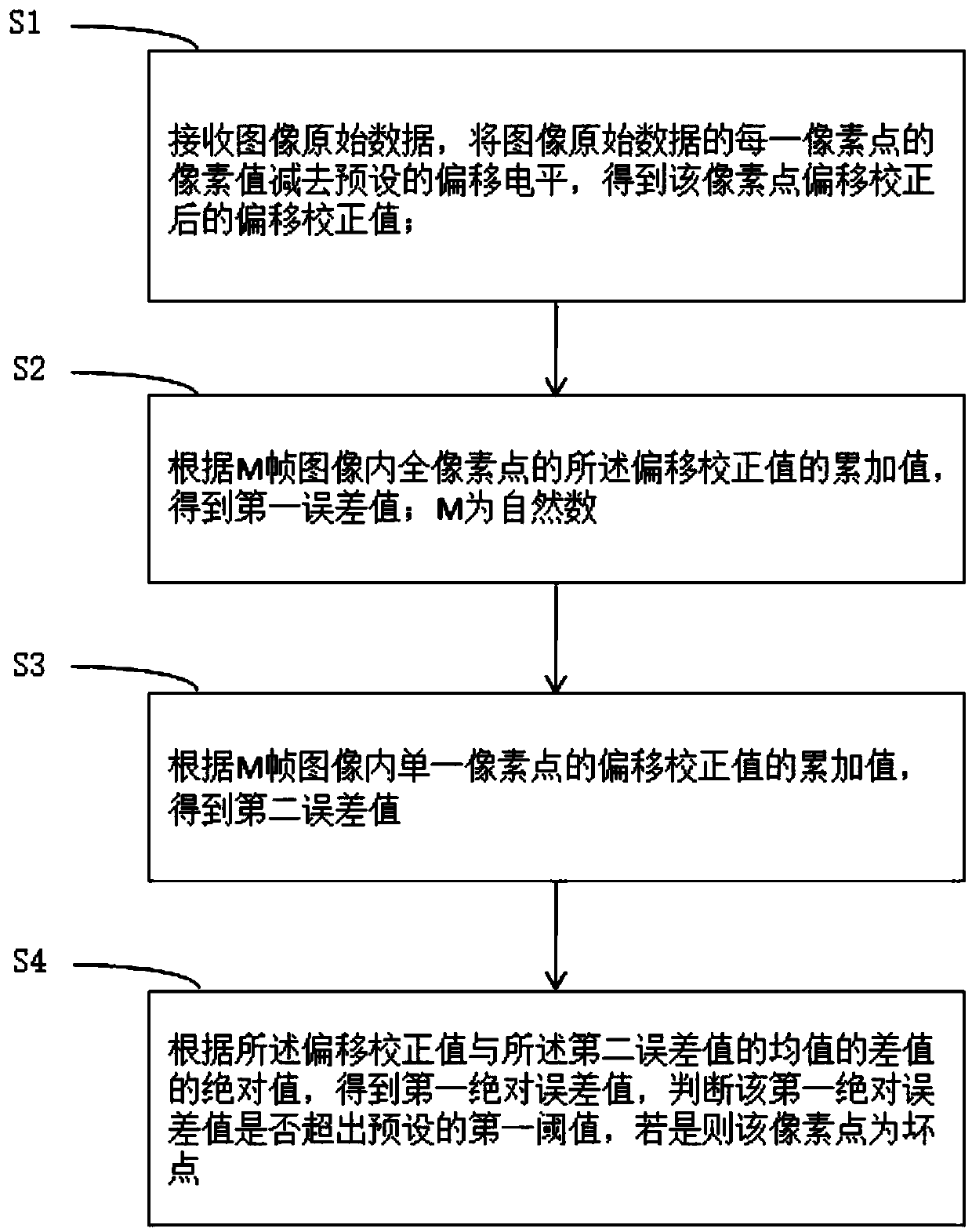
[0025] Such as figure 1 As shown, an embodiment of the present invention provides a method for detecting dead pixels in an image, which includes the steps:

[0026] S1: Receive the original image data, subtract the preset offset level from the pixel value of each pixel of the original image data, to obtain the offset correction value of the pixel point after offset correction;

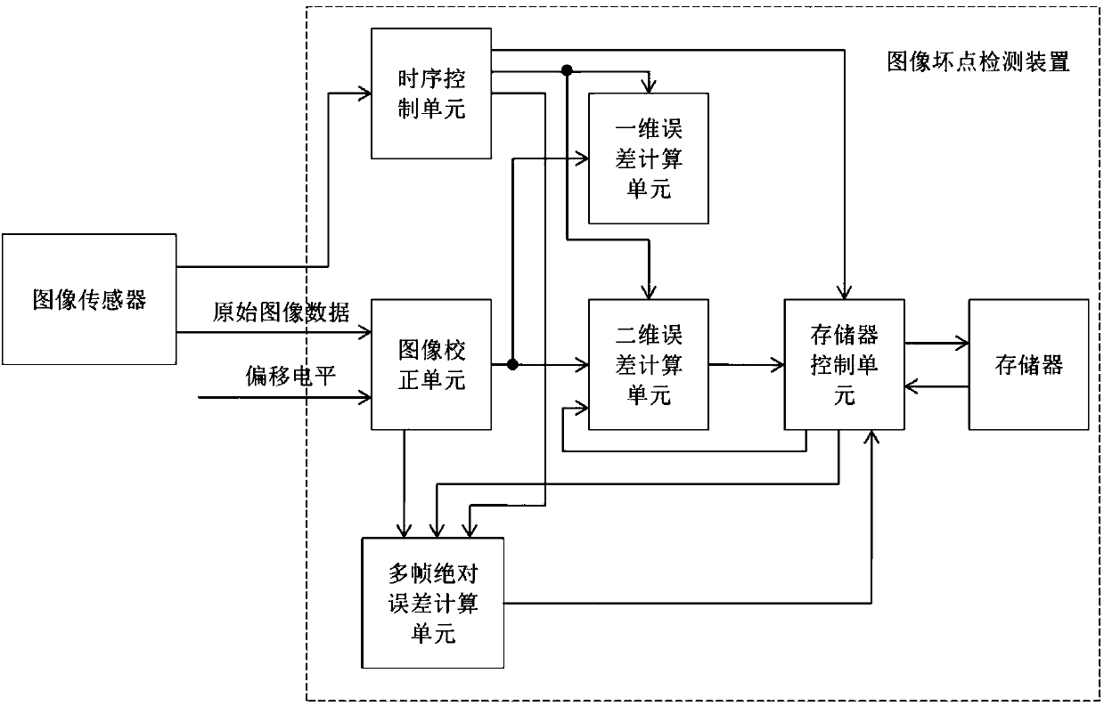
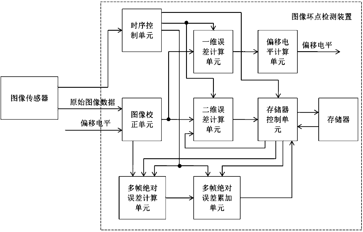
[0027] Specifically, the image sensor collects video images, converts the collected light signals into electrical signals, and converts the electrical signals into pixel values ​​of digital signals, and outputs them to the image defect detection device together with the horizontal synchronization signal and the vertical synchronization signal. In the embodiment of the present invention, the pixel value output by the image sensor is the original image data in the Bayer format.

[0028] In t...


PUM


Abstract

The invention discloses an image defective pixel detection method and device and an image processing chip. The method comprises the steps of receiving image original data and subtracting preset offsetlevel from each pixel value of the image original data, thereby obtaining a offset corrected value after offset correction is carried out on each pixel; acquiring a first error value according to anaccumulated value of the offset corrected values of all pixels in M frames of images; acquiring a second error value according to the accumulated value of the offset corrected values of a single pixelin the M frames of images; and acquiring a first absolute error value according to an absolute value of a difference value between the offset corrected value and the average value of the second errorvalues, and judging whether the pixel is a defective pixel or not according to whether the first absolute error value exceeds a preset first threshold or not. According to the method, the device andthe image processing chip, through calculation of a plurality of intra-frame and interframe pixel errors, the finally obtained error absolute values can accurately reflect whether the pixels are damaged or not and the damage degree.

Description

Technical field [0001] The present invention relates to the technical field of image processing, in particular to a method, a device and an image processing chip for detecting dead pixels of an image. Background technique [0002] With the development of image processing technology, the application of digital video images is becoming more and more common. In the fields of cameras, mobile phones and other mobile devices and vehicles and surveillance, the quality requirements of video images are getting higher and higher. Due to differences in semiconductor manufacturing processes and materials and damage during use, image sensors will have some bad pixels. In order to make the final imaging meet people's visual needs, these bad pixels must be detected and corrected. [0003] The existing bad pixel detection technology mainly uses the neighborhood judgment method, that is, in a frame of image, judge whether the pixel is a bad pixel based on the pixel and the pixels in its surrounding...

Claims


Application Information

Patent Timeline
Patent Type & Authority Applications(China)
IPC IPC(8): H04N17/00G06T7/00
CPCG06T7/0002G06T2207/30168H04N17/004
Inventor 袁扬智刘俊秀韦毅石岭
Owner ARKMICRO TECH
Why Eureka
Try Eureka