Dicarbazole benzene derivative and application thereof and organic electroluminescent device
A technology of dicarbazole benzene and its derivatives, which is applied in the field of organic electroluminescent devices, can solve problems such as difficult flow of electrons, charge imbalance in the light-emitting layer, and reduced device efficiency, and achieve good thermal stability, high luminous purity, and high The effect of luminous efficiency
- Summary
- Abstract
- Description
- Claims
- Application Information
AI Technical Summary
Problems solved by technology
Method used
Image
Examples
Embodiment 1
[0049] Synthesis of compound 3
[0050]
[0051] Synthesis of Intermediate A
[0052] In a flask, add 3-chloro-4-bromo-iodobenzene (20 g, 63 mmol), 9-phenyl-carbazole-3-boronic acid (36 g, 127 mmol), potassium carbonate (18 g, 130 mmol), tetrahydrofuran (300 mL) , water (150mL), tetrakistriphenylphosphine palladium (1g), heated to reflux under nitrogen protection for 12 hours, cooled, extracted with dichloromethane, dried, concentrated, and the crude product was purified by column chromatography to obtain 31g, the yield was 82%.
[0053] Synthesis of compound 3
[0054] In a flask, add intermediate A (2 g, 3.4 mmol), 4-cyanophenylboronic acid (0.74 g, 5.1 mmol), potassium carbonate (1 g, 7 mmol), dioxane (30 mL), water (15 mL), Palladium acetate (0.1g), X-phos (0.2g), heated to reflux under nitrogen protection for 12 hours, cooled, extracted with dichloromethane, dried, concentrated, and the crude product was purified by column chromatography to obtain 1.2g, the yield wa...
Embodiment 9-16
[0060] Fabrication of Organic Electroluminescent Devices
[0061] Preparation of OLEDs using the compounds of the Examples
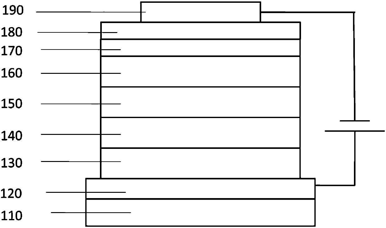
[0062] First, the transparent conductive ITO glass substrate 110 (with the anode 120 on it) (China CSG Group Co., Ltd.) is washed with deionized water, ethanol, acetone and deionized water in sequence, and then treated with oxygen plasma for 30 seconds.
[0063] Then, 3nm thick MnO was evaporated on the ITO 3 (molybdenum oxide) is the hole injection layer 130 .
[0064] Then, 50 nm thick TAPC was deposited on the hole injection layer as the hole transport material 140 .
[0065] Then, TCTA was evaporated to form an electron blocking layer 150 with a thickness of 5 nm.
[0066] Then, a luminescent layer 160 with a thickness of 20nm is vapor-deposited on the electron blocking layer, wherein the compound of the present invention is the host luminescent material, and the weight ratio is 3% Ir(ppy) 3 As a phosphorescent doping guest material.
[0067] Th...
PUM
| Property | Measurement | Unit |
|---|---|---|
| thickness | aaaaa | aaaaa |
Abstract
Description
Claims
Application Information
 - R&D Engineer
- R&D Manager
- IP Professional
- Industry Leading Data Capabilities
- Powerful AI technology
- Patent DNA Extraction
Browse by: Latest US Patents, China's latest patents, Technical Efficacy Thesaurus, Application Domain, Technology Topic, Popular Technical Reports.
© 2024 PatSnap. All rights reserved.Legal|Privacy policy|Modern Slavery Act Transparency Statement|Sitemap|About US| Contact US: help@patsnap.com


