ltps thin film transistor, array substrate and manufacturing method thereof, and display device

A technology for thin film transistors and a manufacturing method, which is applied in the fields of transistors, semiconductor/solid-state device manufacturing, semiconductor devices, etc., can solve the problems of restricting the production capacity of LTPS array substrates, complex processes, and high costs

Active Publication Date: 2021-01-26
BOE TECH GRP CO LTD
View PDF15 Cites 0 Cited by
  • Summary
  • Abstract
  • Description
  • Claims
  • Application Information

AI Technical Summary

Problems solved by technology

However, the existing LTPS array substrates have the problems of complex process and high cost. Compared with traditional a-Si array substrates, which require 4-5 mask processes to manufacture, LTPS array substrates require more than 9 mask processes to manufacture, making The production cost of LTPS array substrates is relatively high and restricts the production capacity of LTPS array substrates

Method used


Image

  • ltps thin film transistor, array substrate and manufacturing method thereof, and display device
  • ltps thin film transistor, array substrate and manufacturing method thereof, and display device
  • ltps thin film transistor, array substrate and manufacturing method thereof, and display device

Examples


Embodiment Construction

[0036] In order to make the technical problems, technical solutions and advantages to be solved by the embodiments of the present invention clearer, the following will describe in detail with reference to the drawings and specific embodiments.

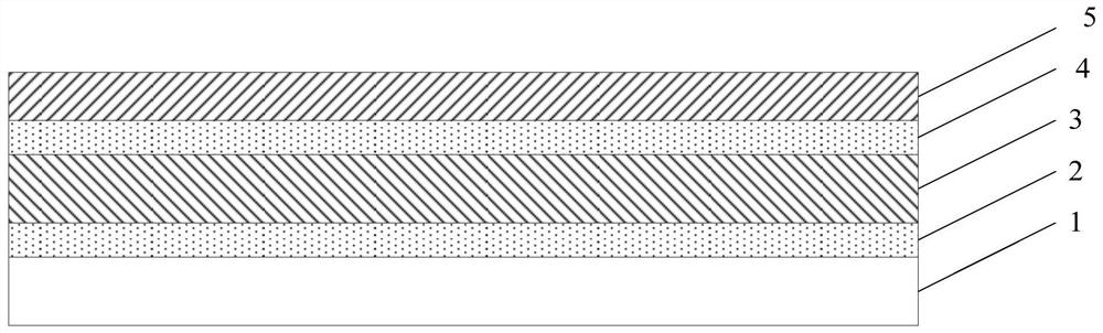
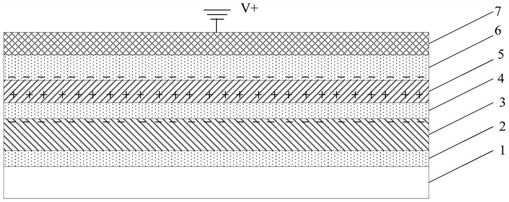
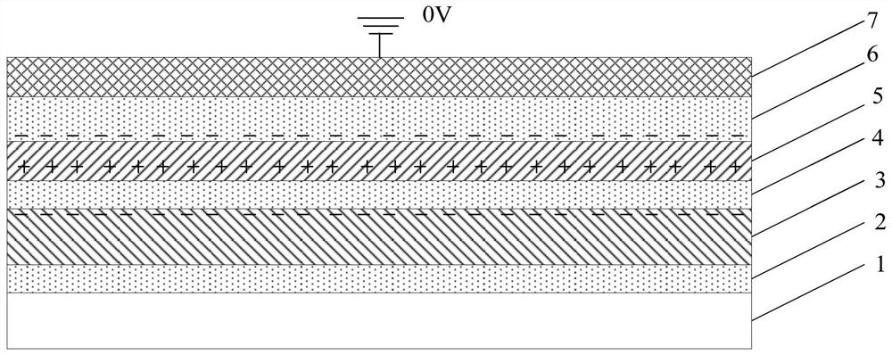
[0037] In the prior art, metal Mo is generally used as a light-shielding pattern to prevent the active layer of the LTPS thin film transistor from being affected by light to affect the device characteristics of the LTPS thin film transistor. Since Mo is a conductor, it cannot be produced with the active layer through a patterning process. It is necessary to pattern the Mo to form a light-shielding pattern, then deposit the buffer layer and the low-temperature polysilicon material, and then pattern the low-temperature polysilicon material to form the pattern of the active layer, so that the LTPS array substrate needs at least 9 Mask processes to manufacture, so that The production cost of the LTPS array substrate is relatively high, whic...


PUM


Abstract

The invention provides an LTPS thin film transistor, an array substrate, a manufacturing method thereof, and a display device, belonging to the field of display technology. Wherein, the manufacturing method of the LTPS thin film transistor includes: forming a light-shielding pattern and the active layer of the LTPS thin film transistor on the base substrate through a patterning process, and the orthographic projection of the active layer on the base substrate falls Into the orthographic projection of the light-shielding pattern on the base substrate, the light-shielding pattern is made of semiconductor material. The technical solution of the invention can reduce the manufacturing cost of the low-temperature polysilicon array substrate, and effectively increase the production capacity of the low-temperature polysilicon array substrate.

Description

technical field [0001] The present invention relates to the field of display technology, in particular to an LTPS thin film transistor, an array substrate and a manufacturing method thereof, and a display device. Background technique [0002] With the development of display technology, LTPS (Low Temperature Poly-silicon, low-temperature polysilicon) backplane technology can realize GOA (Gate Drive on Array, gate integrated drive), etc. due to its high mobility and high aperture ratio. The reason is that the display panel based on this technology has a better display effect than the display panel based on a-Si (amorphous silicon) technology, and is receiving more and more attention. It is also the current small-size LCD (Liquid Crystal Display, An important branch of liquid crystal display). However, the existing LTPS array substrates have the problems of complex process and high cost. Compared with traditional a-Si array substrates, which require 4-5 mask processes to manuf...

Claims


Application Information

Patent Timeline
Patent Type & Authority Patents(China)
IPC IPC(8): H01L29/786H01L21/336
CPCH01L29/66757H01L29/78633G02F1/136209H01L27/1222H01L27/127H01L29/78675G02F1/1368H01L21/0273H01L21/32055H01L27/1288
Inventor 班圣光曹占锋姚琪薛大鹏
Owner BOE TECH GRP CO LTD
Why Eureka
Try Eureka