Array substrate, manufacturing method thereof, and display device

An array substrate, primary color technology, applied in instruments, semiconductor devices, optics, etc., can solve the problems of many patterning times and complex processes, and achieve the effects of high contrast, lower cost, and reduced patterning times

Active Publication Date: 2020-02-07
CHONGQING BOE OPTOELECTRONICS +1
View PDF6 Cites 0 Cited by
  • Summary
  • Abstract
  • Description
  • Claims
  • Application Information

AI Technical Summary

Problems solved by technology

The array substrate structure of the above-mentioned ADS mode requires a large number of patterning times during manufacturing, and the process is relatively complicated.

Method used


Image

  • Array substrate, manufacturing method thereof, and display device
  • Array substrate, manufacturing method thereof, and display device
  • Array substrate, manufacturing method thereof, and display device

Examples


Embodiment Construction

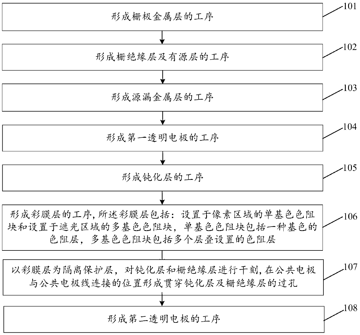
[0033] Embodiments of the present invention provide a method for preparing an array substrate, an array substrate, and a display device, which can fabricate a color filter on the array substrate, reduce the number of patterning times, and reduce costs.

[0034] The following will clearly and completely describe the technical solutions in the embodiments of the present invention with reference to the drawings in the embodiments of the present invention.

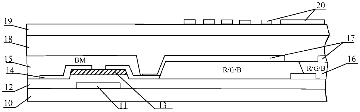
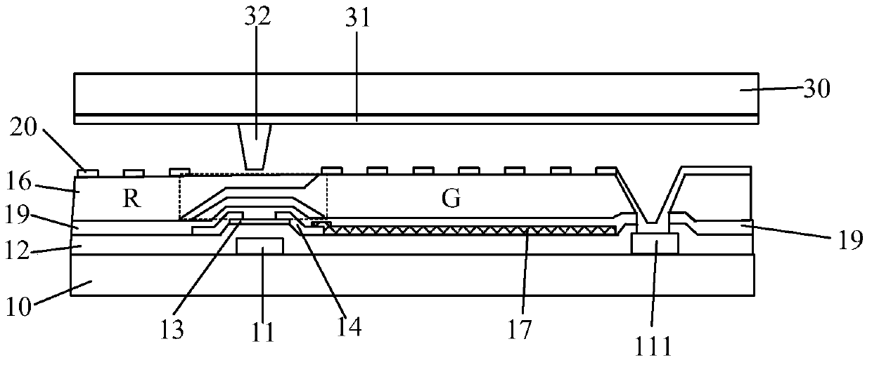
[0035] An embodiment of the present invention provides an array substrate, including: a thin film transistor and a color filter layer disposed on the thin film transistor, and the color filter layer includes: a single-color color-resist block disposed in the pixel area and a color filter block disposed in the light-shielding area The multi-primary-color color-resist block, the single-primary-color color-resist block includes a color-resist layer of one primary color, the multi-primary-color color-resist block includes a plurali...


PUM


Abstract

The invention discloses an array substrate, a preparation method thereof, and a display device, relating to the field of display, capable of fabricating a color filter on the array substrate, reducing the number of patterning times and reducing the cost. The preparation method of the array substrate of the present invention includes: a thin film transistor and a color filter layer arranged on the thin film transistor, and the color filter layer includes: a single primary color color resistance block arranged in the pixel area and a multi-color filter block arranged in the light-shielding area The color-resist block of a primary color includes a color-resist layer of one primary color, and the color-resist block of a multi-primary color includes a plurality of color-resist layers stacked, and each color-resist layer corresponds to a primary color.

Description

technical field [0001] The present invention relates to the display field, in particular to an array substrate, a preparation method thereof, and a display device. Background technique [0002] Due to its advantages of light weight, low power consumption, low radiation, and a large amount of space saving, liquid crystal displays have replaced traditional cathode ray tube displays and are widely used in various display fields, such as households, public places, offices, and personal electronics. products etc. [0003] The current manufacturing process of liquid crystal panels is to separately manufacture the array (Array) substrate and the color filter (Color Filter) substrate, and then align the array substrate and the color filter substrate to form a cell (Cell). However, when the array substrate and the color filter substrate are aligned to form a box, due to the limitation of alignment accuracy, alignment deviation is very easy to occur, and alignment deviation will caus...

Claims


Application Information

Patent Timeline
Patent Type & Authority Patents(China)
IPC IPC(8): G02F1/1362G02F1/1335
CPCG02F1/133514G02F1/1362G02F1/136231G02F1/136222G02F1/136209H01L27/1248G02F1/134345G02F1/1335G02F1/133516G02F1/13394G02F1/134309G02F1/13439G02F1/136227G02F1/136286G02F1/1368G02F2201/121G02F2201/124H01L27/124H01L27/1262H01L27/1288
Inventor 余道平金熙哲
Owner CHONGQING BOE OPTOELECTRONICS
Why Eureka
Try Eureka