Double-faced alumina P-type PERC solar cell and making method
A technology of solar cells and manufacturing methods, applied in the field of solar cells, can solve problems such as increased production costs, and achieve the effects of improving conversion efficiency and reducing reflectivity
- Summary
- Abstract
- Description
- Claims
- Application Information
AI Technical Summary
Problems solved by technology
Method used
Image
Examples
Embodiment 1
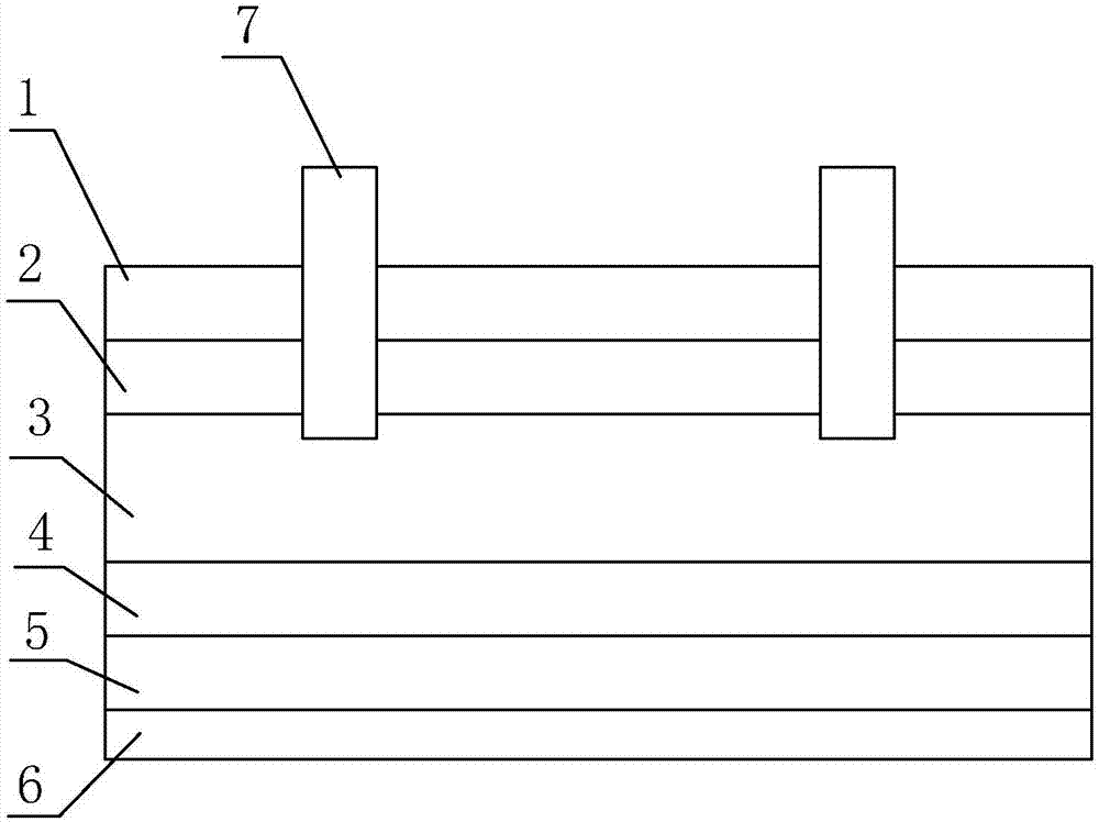
[0028] Such as figure 1 As shown, a double-sided alumina P-type PERC solar cell includes a silicon wafer 3 and two positive electrodes 7 arranged on the front side of the silicon wafer; the front side of the silicon wafer is sequentially provided with a front silicon nitride film 2 and a front surface An aluminum oxide film 1; a back aluminum oxide film 4, a back silicon nitride film 5, and a back electrode / field 6 are sequentially provided on the back of the silicon wafer.
[0029] 1) Cleaning and texturing: After cleaning the P-type silicon wafer with hydrogen peroxide, place it in an alkali with a temperature of 80°C and a concentration of 3% for texturing for 15 minutes, then wash it with hydrochloric acid and hydrofluoric acid for 2 minutes, wash it with pure water for 2 minutes, and then bake it Dry.
[0030] 2) Diffusion to make PN junction: pass the silicon wafer after step 1) into texture at 840°C under the high temperature condition of 840°C, and pass phosphorus oxy...
Embodiment 2
[0044] A double-sided aluminum oxide P-type PERC solar cell, comprising a silicon wafer 3 and two positive electrodes 7 arranged on the front side of the silicon wafer; the front side of the silicon wafer is provided with a front silicon nitride film 2 and a front aluminum oxide film in sequence 1. The back of the silicon wafer is provided with an aluminum oxide film 4 on the back, a silicon nitride film 5 on the back, and a back electrode / field 6 in sequence.
[0045] The manufacturing method of the double-sided aluminum oxide P-type PERC solar cell comprises the following steps:
[0046] 1) Cleaning and texturing: After cleaning the P-type silicon wafer with hydrogen peroxide, place it in 3% alkali at 78°C for 20 minutes, then wash it with hydrochloric acid and hydrofluoric acid for 3 minutes, wash it with pure water for 3 minutes, and then dry it .
[0047] 2) Diffusion PN junction: the silicon wafer after step 1) is textured at 720° C., and phosphorus oxychloride, nitroge...
Embodiment 3
[0055] A double-sided aluminum oxide P-type PERC solar cell, comprising a silicon wafer 3 and two positive electrodes 7 arranged on the front side of the silicon wafer; the front side of the silicon wafer is provided with a front silicon nitride film 2 and a front aluminum oxide film in sequence 1. The back of the silicon wafer is provided with an aluminum oxide film 4 on the back, a silicon nitride film 5 on the back, and a back electrode / field 6 in sequence.
[0056] The manufacturing method of the double-sided aluminum oxide P-type PERC solar cell comprises the following steps:
[0057] 1) Cleaning and texturing: After cleaning the P-type silicon wafer with hydrogen peroxide, place it in 4% alkali at 82°C for 10 minutes, then wash it with hydrochloric acid and hydrofluoric acid for 1 minute, wash it with pure water for 1 minute, and then dry it .
[0058] 2) Diffusion to make PN junction: pass the silicon wafer after step 1) textured at 850°C into phosphorus oxychloride, n...
PUM
| Property | Measurement | Unit |
|---|---|---|
| thickness | aaaaa | aaaaa |
| thickness | aaaaa | aaaaa |
| thickness | aaaaa | aaaaa |
Abstract
Description
Claims
Application Information
 - R&D
- Intellectual Property
- Life Sciences
- Materials
- Tech Scout
- Unparalleled Data Quality
- Higher Quality Content
- 60% Fewer Hallucinations
Browse by: Latest US Patents, China's latest patents, Technical Efficacy Thesaurus, Application Domain, Technology Topic, Popular Technical Reports.
© 2025 PatSnap. All rights reserved.Legal|Privacy policy|Modern Slavery Act Transparency Statement|Sitemap|About US| Contact US: help@patsnap.com


