Semiconductor device manufacturing method and substrate processing apparatus

A technology of a substrate processing device and a manufacturing method, which is applied in the fields of semiconductor/solid-state device manufacturing, semiconductor/solid-state device testing/measurement, transistors, etc., can solve problems such as uneven substrate processing results, and achieve the effect of improving processing uniformity

Active Publication Date: 2022-06-21
KOKUSA ELECTRIC CO LTD
View PDF6 Cites 0 Cited by
  • Summary
  • Abstract
  • Description
  • Claims
  • Application Information

AI Technical Summary

Problems solved by technology

[0006] There is a problem that the processing result of each substrate is not uniform due to individual differences of the devices even if the respective monitoring values ​​of the devices fall within the reference values

Method used


Image

  • Semiconductor device manufacturing method and substrate processing apparatus
  • Semiconductor device manufacturing method and substrate processing apparatus
  • Semiconductor device manufacturing method and substrate processing apparatus

Examples


Embodiment Construction

[0034] Embodiments disclosed in the present invention will be described below.

[0035]

[0036] Hereinafter, one embodiment disclosed by the present invention will be described with reference to the drawings.

[0037] The substrate processing system of this embodiment will be described below.

[0038] (1) Structure of the substrate processing system

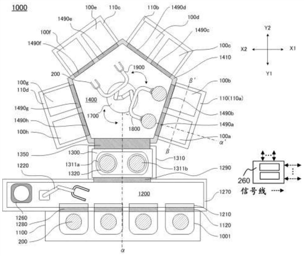
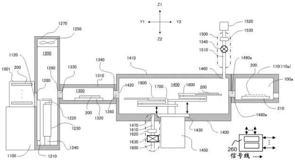
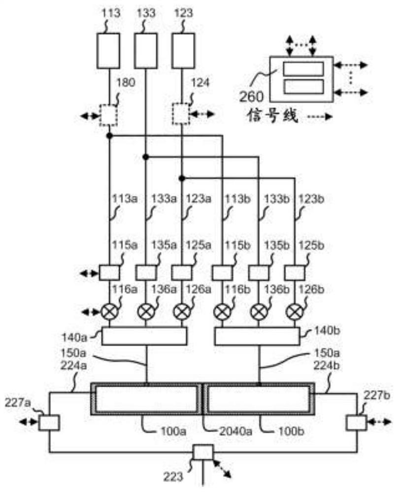
[0039] use figure 1 , figure 2 , image 3 A schematic configuration of a substrate processing system according to an embodiment will be described. figure 1 is a cross-sectional view showing a configuration example of the substrate processing system of this embodiment. figure 2 shows a configuration example of the substrate processing system of this embodiment figure 1 α-α' longitudinal section view. image 3 Yes figure 1 The β-β' vertical cross-sectional view in the figure is an explanatory diagram illustrating the gas supply system and exhaust system supplied to the processing module.

[0040] exist figure 1 and ...


PUM


Abstract

The present invention provides a method of manufacturing a semiconductor device and a substrate processing apparatus, and its technical subject is to improve the uniformity of processing for each substrate. The manufacturing method of a semiconductor device has: a step of operating a processing device based on a first processing setting to process a substrate; a step of acquiring device data of the processing device during processing; a step of generating first evaluation data of the processing device; a step of determining a recipe item executable in the processing device based on the first evaluation data; and a step of reporting the recipe item.

Description

technical field [0001] The present invention discloses a recording medium, a program, a manufacturing method of a semiconductor device, and a substrate processing apparatus. Background technique [0002] With the high integration of semiconductor devices represented by large-scale integrated circuit (Large Scale Integrated Circuit, hereinafter referred to as "LSI"), DRAM (Dynamic Random Access Memory: dynamic random access memory), flash memory (Flash Memory), etc., The refinement of circuit patterns and structures formed during the manufacturing process is being advanced. In the substrate processing equipment that performs one of the manufacturing processes of semiconductor devices, FDC (Fault Detection & Classification: Fault Detection & Classification) is performed based on the stored monitoring data, the soundness of the equipment is confirmed, and the abnormality is notified by an alarm. This prevents substandard production. For example, it is described in Patent Docu...

Claims


Application Information

Patent Timeline
Patent Type & Authority Patents(China)
IPC IPC(8): H01L21/67
CPCH01L21/67253H01J37/32899H01J37/32926H01J37/3476H01L21/67242H01L22/12H01L22/14H01L22/20H01L22/34H10B12/00Y02P90/02H01L22/26
Inventor 中山雅则寺崎正
Owner KOKUSA ELECTRIC CO LTD
Why Eureka
Try Eureka