Internal super-thick copper plate laminating method
A technology of thick copper plate and inner layer, applied in the direction of multi-layer circuit manufacturing, printed circuit, electrical components, etc., can solve the problems of bubble circuit, circuit whitening, whitening, etc., to improve glue filling and poor fiber cutting, and ensure quality Effect
- Summary
- Abstract
- Description
- Claims
- Application Information
AI Technical Summary
Problems solved by technology
Method used
Image
Examples
Embodiment
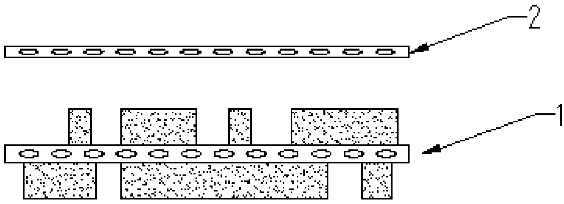
[0035] This embodiment discloses a lamination method of an inner layer ultra-thick copper plate, Figure 3-4 It is the operating principle diagram of the inner layer ultra-thick copper plate lamination method in the present invention, and the specific operation process of the inner layer ultra-thick copper plate lamination method is as follows:
[0036] S1, send out materials, select the substrate;
[0037] S2, the inner layer, making an inner layer circuit on the substrate to form an inner layer circuit board;
[0038] S3, drilling positioning holes, drilling positioning holes on the inner circuit board;
[0039] S4, browning, browning the inner layer circuit board after the positioning hole is drilled;
[0040] S5. Resin printing, resin printing is performed on the surface of the inner circuit board after step S4, the resin fills the upper and lower surfaces of the inner circuit board, and the inner circuit board needs to be printed before resin printing carry out roastin...
PUM
 Abstract
Description
Claims
Application Information
 - R&D
- Intellectual Property
- Life Sciences
- Materials
- Tech Scout
- Unparalleled Data Quality
- Higher Quality Content
- 60% Fewer Hallucinations
Browse by: Latest US Patents, China's latest patents, Technical Efficacy Thesaurus, Application Domain, Technology Topic, Popular Technical Reports.
© 2025 PatSnap. All rights reserved.Legal|Privacy policy|Modern Slavery Act Transparency Statement|Sitemap|About US| Contact US: help@patsnap.com


