A kind of LED encapsulation method

A LED package, hemispherical technology, applied in the direction of semiconductor devices, electrical components, circuits, etc., can solve the problems of insufficient contact between the bottom surface of the heat sink, affecting the heat dissipation effect, and reducing the light intensity, so as to suppress the total reflection effect and improve heat convection speed, improving the effect of luminous dispersion

Active Publication Date: 2020-12-22
INST OF FLEXIBLE ELECTRONICS TECH OF THU ZHEJIANG
View PDF5 Cites 0 Cited by
  • Summary
  • Abstract
  • Description
  • Claims
  • Application Information

AI Technical Summary

Problems solved by technology

Since the chip absorbs backscattered light, this direct coating method will reduce the light extraction efficiency of the package. In addition, the high temperature generated by the chip will significantly reduce the quantum efficiency of the phosphor, which will seriously affect the Package Lumen Efficiency
Secondly, the light emitted by the LED light source is generally distributed in a divergent manner, resulting in insufficient illumination brightness of the light source. Generally, secondary shaping is required through an external lens to meet the lighting needs of specific occasions, thus increasing production costs.
Thirdly, because high-power LEDs are used in lighting and other occasions, cost control is very important, and the structural size of the external heat sink of high-power LED lamps is not allowed to be too large, and it is impossible to allow active cooling by adding electric fans and other methods. The safe junction temperature should be within 110°C. If the junction temperature is too high, it will lead to a series of problems such as reduced light intensity, spectral shift, increased color temperature, increased thermal stress, and accelerated chip aging, which greatly reduces the service life of the LED. At the same time, it can also lead to accelerated aging of the encapsulation gel filled on the chip, affecting its light transmission efficiency
At present, most of the chips are packaged on thin metal heat dissipation substrates. Because metal heat dissipation substrates are thin, have small heat capacity, and are easy to deform, the contact between them and the bottom surface of the heat sink is not close enough to affect the heat dissipation effect.

Method used


Image

  • A kind of LED encapsulation method
  • A kind of LED encapsulation method
  • A kind of LED encapsulation method

Examples


Embodiment 1

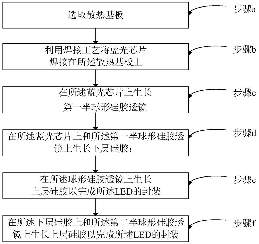
[0054] See figure 1 , figure 1 It is a flow chart of an LED packaging method provided by an embodiment of the present invention. The method comprises the steps of:

[0055]Step a, selecting a heat dissipation substrate;

[0056] Step b, using a welding process to weld the blue light chip on the heat dissipation substrate;

[0057] Step c, growing a first hemispherical silica gel lens on the blue chip;

[0058] Step d, growing a lower layer of silica gel on the blue light chip and the first hemispherical silica gel lens;

[0059] Step e, growing a second hemispherical silica gel lens on the lower layer of silica gel;

[0060] Step f, growing an upper layer of silica gel on the lower layer of silica gel and the second hemispherical silica gel lens to complete the packaging of the LED.

[0061] Preferably, the heat dissipation substrate is made of iron and has a thickness of 0.5-10mm.

[0062] Preferably, a circular through hole is provided in the heat dissipation substrat...

Embodiment 2

[0091] See figure 2 , figure 2 It is a schematic flow chart of an LED packaging method provided by an embodiment of the present invention. On the basis of the above embodiments, this embodiment will introduce the process flow of the present invention in more detail. The method includes:

[0092] S1, preparation of heat dissipation substrate;

[0093] S11, preparation of support / radiation substrate;

[0094] Specifically, select a heat dissipation substrate 101 with a thickness of 0.5-10 mm and a material of iron, and cut the heat dissipation substrate 101;

[0095] S12. Cleaning of the support / heat dissipation substrate;

[0096] Specifically, clean the stains on the heat dissipation substrate 101 and the support, especially the oil stains;

[0097] S13, baking of the bracket / radiation substrate;

[0098] Specifically, the cleaned heat dissipation substrate 101 and the support are baked to keep the heat dissipation substrate 101 and the support dry.

[0099] Preferab...

Embodiment 3

[0136] Please also see image 3 , Figure 4 , Figure 5 and Figure 6a ~ Figure 6b , image 3 A schematic cross-sectional view of an LED package structure provided by an embodiment of the present invention, Figure 4 A schematic cross-sectional view of a heat dissipation substrate provided by an embodiment of the present invention, Figure 5 A schematic cross-sectional view of a Blu-ray chip provided by an embodiment of the present invention, Figure 6a A schematic cross-sectional view of a hemispherical silicone lens provided in an embodiment of the present invention, Figure 6b A cross-sectional schematic diagram of another hemispherical silicone lens provided by an embodiment of the present invention. On the basis of the above embodiments, this embodiment will introduce the LED packaging structure of the present invention, and the LED packaging structure includes:

[0137] heat dissipation substrate 101;

[0138] Among them, such as Figure 4 As shown, the material...


PUM

PropertyMeasurementUnit
thicknessaaaaaaaaaa
diameteraaaaaaaaaa
thicknessaaaaaaaaaa

Abstract

The invention relates to an LED packaging method. The method comprises steps: a cooling substrate is selected; a blue light chip is welded on the cooling substrate by using a welding technology; a first hemispherical silica gel lens grows on the blue light chip; a lower silica gel layer grows on the blue light chip and the first hemispherical silica gel lens; a second hemispherical silica gel lensgrows on the lower silica gel layer; and an upper silica gel layer grows on the lower silica gel layer and the second hemispherical silica gel lens to complete LED packaging. According to the LED packaging structure of the invention, through adopting the iron cooling substrate with an oblique through hole structure, the cooling effects of the LED are increased; through adopting the spherical silica gel lens structure, light of the LED chip can shine out better through the packaging material, and the light transmittance is improved.

Description

technical field [0001] The invention relates to the technical field of LED packaging, in particular to an LED packaging method. Background technique [0002] The first batch of LED light-emitting diodes that appeared on the market in the middle of the 20th century have made remarkable progress after decades of progress. Its luminous efficiency has reached the level of thermal radiation light source, its light intensity has reached candlelight level, and its radiation color is rich. Especially the birth of white light LED, the application of LED products in the field of lighting has become a very influential new product. [0003] LED uses the electrons and holes in the semiconductor material to combine with each other and release energy, so that the energy band level changes, and the released energy is displayed by luminescence. LED has the advantages of small size, long life, low driving voltage, low power consumption, fast response rate, good shock resistance, etc., and is...

Claims


Application Information

Patent Timeline
Patent Type & Authority Patents(China)
IPC IPC(8): H01L33/00H01L33/54H01L33/58H01L33/64
CPCH01L33/005H01L33/54H01L33/58H01L33/641H01L33/642
Inventor 尹晓雪
Owner INST OF FLEXIBLE ELECTRONICS TECH OF THU ZHEJIANG
Why Eureka
Try Eureka