A flat terminal passivation method and semiconductor power device

A technology for power devices and semiconductors, applied in the field of planar terminal passivation methods and semiconductor power devices, can solve the problems of inability to prevent electron accumulation in passivation layers and contamination of impurity ions, reducing reliability of semiconductor power devices, mismatch of expansion coefficients, and the like, Achieve high mechanical properties, stable breakdown voltage and leakage current, and not easy to fall off

Active Publication Date: 2020-11-03
GLOBAL ENERGY INTERCONNECTION RES INST CO LTD +2
View PDF2 Cites 0 Cited by
  • Summary
  • Abstract
  • Description
  • Claims
  • Application Information

AI Technical Summary

Problems solved by technology

[0004] 2. When the silicon dioxide film is used as a passivation layer, it cannot prevent electron accumulation and impurity ion pollution in the passivation layer
However, the thermal expansion effect of polyimide is low. When the semiconductor power device covered with polyimide on the planar terminal works in a high temperature and high pressure environment, the expansion coefficient of polyimide may not match the expansion coefficient of the planar terminal material. The problem, which in turn leads to polyimide falling off, reduces the reliability of semiconductor power devices

Method used


Image

  • A flat terminal passivation method and semiconductor power device
  • A flat terminal passivation method and semiconductor power device
  • A flat terminal passivation method and semiconductor power device

Examples


Embodiment Construction

[0044] In order to make the purpose, technical solutions and advantages of the embodiments of the present invention more clear, the technical solutions in the embodiments of the present invention will be clearly and completely described below in conjunction with the accompanying drawings in the embodiments of the present invention. Obviously, the described embodiments It is a part of embodiments of the present invention, but not all embodiments. Based on the embodiments of the present invention, all other embodiments obtained by persons of ordinary skill in the art without making creative efforts belong to the protection scope of the present invention.

[0045] A method for passivating a planar terminal provided by an embodiment of the present invention will be described below with reference to the accompanying drawings.

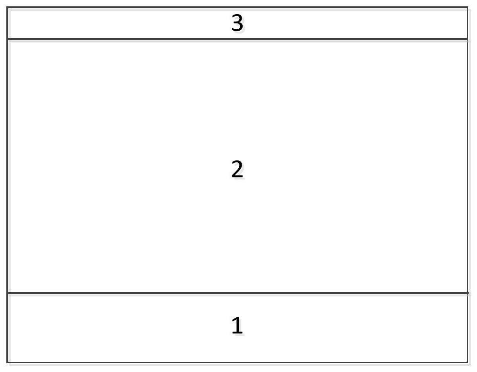
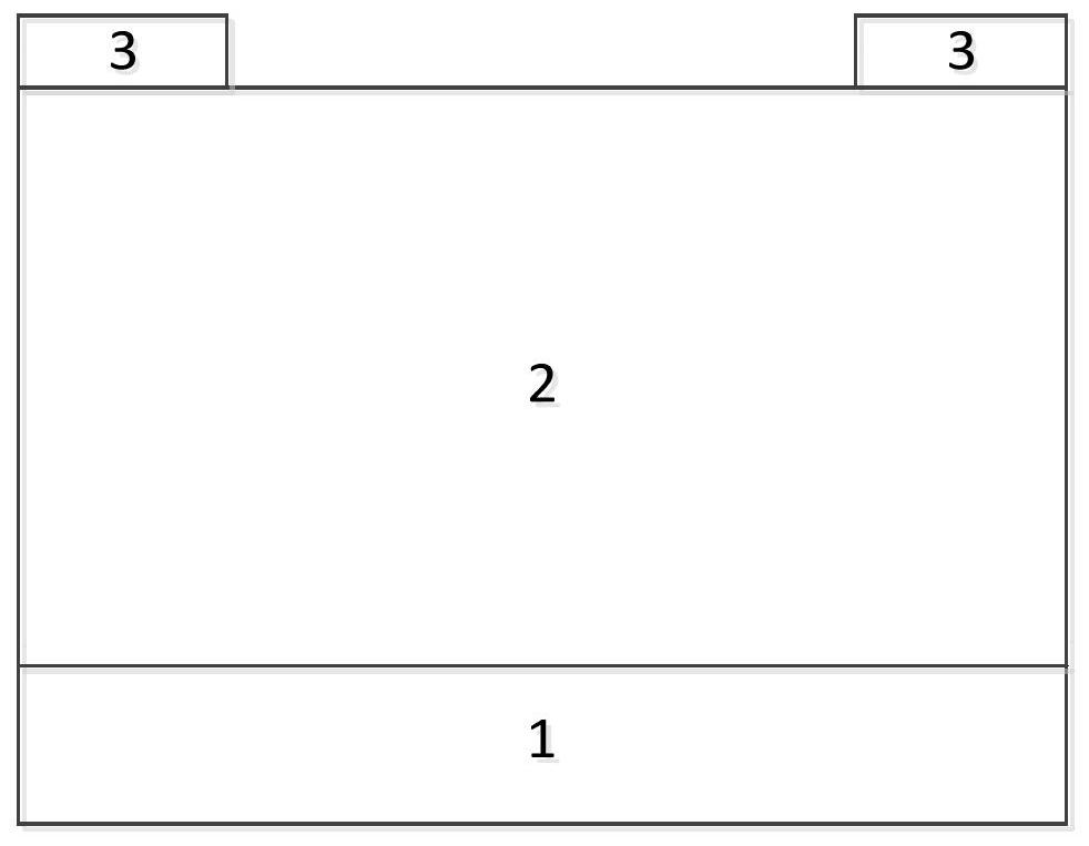
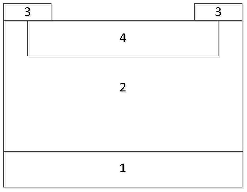
[0046] In this embodiment, a multilayer composite passivation layer is formed by sequentially depositing a dielectric layer, a glass passivation layer and a...


PUM

PropertyMeasurementUnit
thicknessaaaaaaaaaa

Abstract

The invention provides a planar terminal passivation method and a semiconductor power device. The method includes sequentially depositing a dielectric layer, a glass passivation layer and a polyimide protective layer on the semiconductor power device to form a multilayer composite passivation layer; the semiconductor power device is manufactured by the above-mentioned method. Compared with the prior art, the present invention provides a planar terminal passivation method and semiconductor power device, which can improve the sealing performance of the semiconductor power device by adopting a multi-layer composite passivation layer, prevent harmful impurity ions from diffusing to the substrate surface, and at the same time The use of a glass passivation layer can reduce the requirements on the thickness and expansion coefficient of the polyimide protective layer, so that the semiconductor power device has high mechanical properties and is not easy to fall off when it works in a high temperature environment.

Description

technical field [0001] The invention relates to the technical field of semiconductor power device preparation, in particular to a planar terminal passivation method and a semiconductor power device. Background technique [0002] Semiconductor power devices are widely used in industrial processing, household appliances, transportation, smart grid, national defense military equipment, aerospace and other fields. The terminals are generally planar terminals manufactured by planar technology, but the silicon dioxide near the substrate The film also has the following defects: [0003] 1. There are fixed charges in the silicon dioxide film: if the semiconductor power device is an n-type semiconductor power device, electron accumulation will occur; if the semiconductor power device is a p-type semiconductor power device, an inversion layer will be formed; [0004] 2. When the silicon dioxide film is used as a passivation layer, it cannot prevent electron accumulation and impurity ...

Claims


Application Information

Patent Timeline
Patent Type & Authority Patents(China)
IPC IPC(8): H01L21/56H01L23/29H01L23/31
CPCH01L21/56H01L23/291H01L23/293H01L23/3192H01L2224/02166H01L2224/05H01L2224/02126
Inventor 温家良吴迪金锐刘钺杨何延强徐哲潘艳
Owner GLOBAL ENERGY INTERCONNECTION RES INST CO LTD
Why Eureka
Try Eureka