Non-refrigerated infrared imaging sensor based on super surface and preparation method thereof
An uncooled infrared and imaging sensor technology, used in instruments, scientific instruments, radiation pyrometry, etc., can solve the problems of inability to achieve target band absorption, difficulty in improving process realization, and difficulty in controlling the height of resonant cavity, and achieve the goal of improving detection. The ability to increase the difficulty of the process, the effect of low additional heat capacity
- Summary
- Abstract
- Description
- Claims
- Application Information
AI Technical Summary
Problems solved by technology
Method used
Image
Examples
Embodiment 1
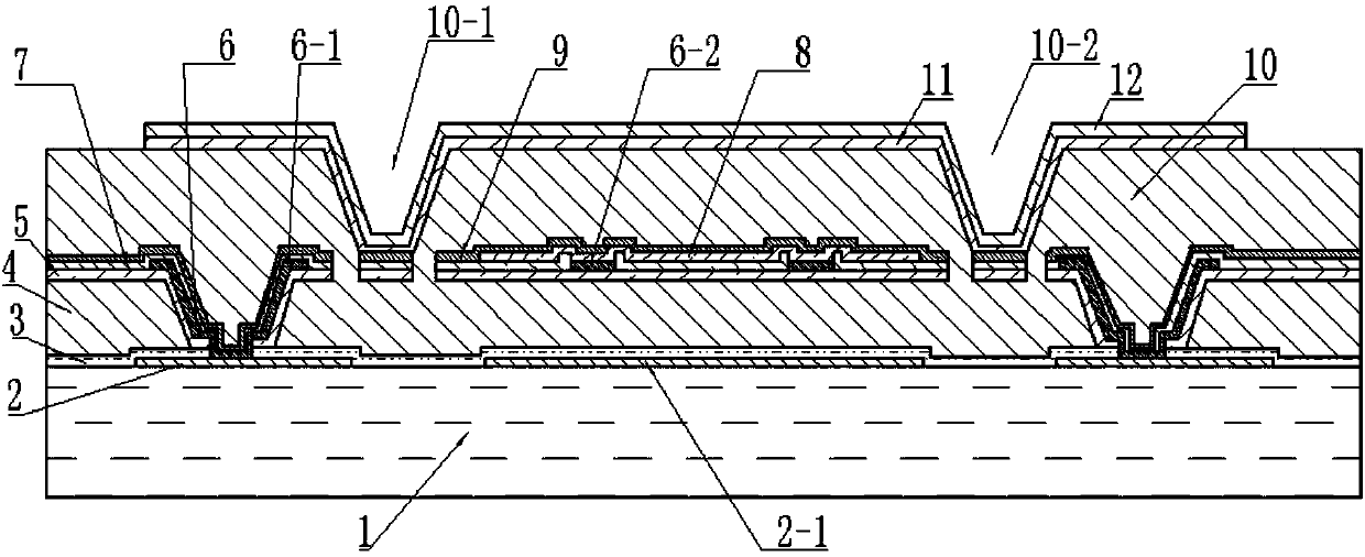
[0069] Such as Figure 1-6 As shown, a metasurface-based uncooled infrared imaging sensor includes a double-layer uncooled infrared detector, and the double-layer uncooled infrared detector includes a semiconductor substrate 1 containing a readout circuit and a microbridge support structure The detector body, the detector body includes a first layer of suspended structure and a second layer of suspended structure, the second layer of suspended structure is arranged on the first layer of suspended structure, and the first layer of suspended structure includes a metal reflective layer 2 , an insulating medium layer 3, a metal electrode layer 6, an electrode protection layer 7, a first support layer 5, a heat-sensitive protection layer 9 and a heat-sensitive layer 8, and the second suspended structure includes a metamaterial support layer 11 and is arranged on the The metamaterial support layer 11 and the metamaterial support protection layer 12 are provided with a metamaterial s...
Embodiment 2
[0075] The difference from Implementation 1 is that, as in Figure 7 As shown, the outer contour of the metamaterial structure 13 is rectangular, the center is provided with a rectangular hollow 13-6, the outer contour is provided with a horizontal centerline and a vertical centerline, the rectangular hollow 13-6 and the A thin strip 13-5 that is bent back and forth to form a closed-loop structure is provided between the outer contours. The closed-loop structure formed by the thin strip 13-5 is symmetrical about the horizontal centerline and the vertical centerline respectively. The closed-loop structure The bending part is a right-angle bending, and the material of the thin strip is NiCr, the thickness is 20nm, and the width is 0.5 μm-5 μm.
Embodiment 3
[0077] The difference from Example 1 is that, as Figure 8-Figure 9 As shown, the metamaterial structure 13 includes a rectangular outline formed by a flat strip 13-7, and the center of each side of the rectangular outline is provided with an inward U-shaped bend 13-8, and the flat strip 13- The material of 7 is NiCr, the thickness is 20nm, and the width is 0.5μm-5μm.
PUM
| Property | Measurement | Unit |
|---|---|---|
| Thickness | aaaaa | aaaaa |
| Thickness | aaaaa | aaaaa |
| Thickness | aaaaa | aaaaa |
Abstract
Description
Claims
Application Information
 - R&D
- Intellectual Property
- Life Sciences
- Materials
- Tech Scout
- Unparalleled Data Quality
- Higher Quality Content
- 60% Fewer Hallucinations
Browse by: Latest US Patents, China's latest patents, Technical Efficacy Thesaurus, Application Domain, Technology Topic, Popular Technical Reports.
© 2025 PatSnap. All rights reserved.Legal|Privacy policy|Modern Slavery Act Transparency Statement|Sitemap|About US| Contact US: help@patsnap.com


