Preparation method of GaN epitaxial structure taking hexagonal BN-graphene composite layer as buffer layer
A graphene composite and hexagonal boron nitride technology, which is applied in the field of optoelectronics, can solve the problems such as difficult to control growth conditions, achieve good thickness controllability, alleviate lattice mismatch, and simple equipment
- Summary
- Abstract
- Description
- Claims
- Application Information
AI Technical Summary
Problems solved by technology
Method used
Image
Examples
Embodiment 1
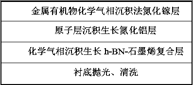
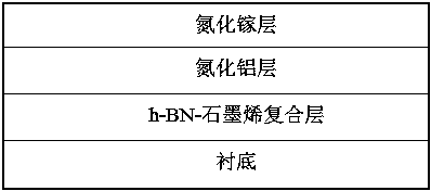
[0039] A method for preparing a gallium nitride epitaxial structure based on a hexagonal boron nitride-graphene composite layer as a buffer layer, comprising the following process steps:
[0040] A, polishing and cleaning the copper substrate;
[0041] B, grow h-BN-graphene composite layer on copper substrate;
[0042]C, utilize atomic layer deposition to grow a layer of aluminum nitride layer on the h-BN-graphene composite layer;
[0043] D. A gallium nitride layer is grown on the thin aluminum nitride layer by metal-organic chemical vapor deposition.
Embodiment 2
[0045] A method for preparing a gallium nitride epitaxial structure based on a hexagonal boron nitride-graphene composite layer as a buffer layer, comprising the following process steps:
[0046] A, polishing and cleaning the copper substrate;
[0047] B, grow h-BN-graphene composite layer on copper substrate;
[0048] C, utilize atomic layer deposition to grow a layer of aluminum nitride layer on the h-BN-graphene composite layer;
[0049] D. A gallium nitride layer is grown on the thin aluminum nitride layer by metal-organic chemical vapor deposition.
[0050] In step A, specifically:
[0051] Firstly, the copper substrate was cleaned to remove the oil and oxide layer on the surface, and then after double polishing by mechanical polishing and electrochemical polishing, it was washed three times with ethanol and deionized water in turn, washed with dilute hydrochloric acid for 5 minutes, cleaned with deionized water, and blown with nitrogen. Dry to obtain a copper substrat...
Embodiment 3
[0053] A method for preparing a gallium nitride epitaxial structure based on a hexagonal boron nitride-graphene composite layer as a buffer layer, comprising the following process steps:
[0054] A, polishing and cleaning the copper substrate;
[0055] B, grow h-BN-graphene composite layer on copper substrate;
[0056] C, utilize atomic layer deposition to grow a layer of aluminum nitride layer on the h-BN-graphene composite layer;
[0057] D. A gallium nitride layer is grown on the thin aluminum nitride layer by metal-organic chemical vapor deposition.
[0058] In step A, specifically:
[0059] Firstly, the copper substrate was cleaned to remove the oil stain and oxide layer on the surface, and after the double polishing of mechanical polishing and electrochemical polishing, it was washed three times with ethanol and deionized water in turn, washed with dilute hydrochloric acid for 10 minutes, washed with deionized water, and blown with nitrogen. Dry to obtain a copper sub...
PUM
| Property | Measurement | Unit |
|---|---|---|
| thickness | aaaaa | aaaaa |
| thickness | aaaaa | aaaaa |
| lattice constant | aaaaa | aaaaa |
Abstract
Description
Claims
Application Information
 - R&D
- Intellectual Property
- Life Sciences
- Materials
- Tech Scout
- Unparalleled Data Quality
- Higher Quality Content
- 60% Fewer Hallucinations
Browse by: Latest US Patents, China's latest patents, Technical Efficacy Thesaurus, Application Domain, Technology Topic, Popular Technical Reports.
© 2025 PatSnap. All rights reserved.Legal|Privacy policy|Modern Slavery Act Transparency Statement|Sitemap|About US| Contact US: help@patsnap.com


