Wavelength conversion device and preparing method thereof, luminescent device and projection device
A wavelength conversion device and a technology of luminescent ceramics, which are applied in the fields of lighting and projection, can solve the problems of reduced excitation light utilization efficiency, low luminous brightness of light source, low collection rate of optical system, etc., so as to improve wavelength conversion efficiency, high heat dissipation efficiency, high brightness effect
- Summary
- Abstract
- Description
- Claims
- Application Information
AI Technical Summary
Problems solved by technology
Method used
Image
Examples
Embodiment 1
[0061] see figure 2 , figure 2 It is a structural schematic diagram of Embodiment 1 of the present invention. Such as figure 2 As shown, the wavelength conversion device is composed of a first luminescent ceramic layer 11 , a second luminescent ceramic layer 12 and a reflective layer 13 stacked in sequence.
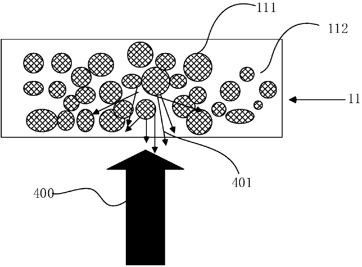
[0062] In this embodiment, the first luminescent ceramic layer 11 is a transparent luminescent ceramic layer, and the first luminescent ceramic layer 11 includes first luminescent ceramic grains 111; the first luminescent ceramic grains are garnet luminescent ceramic grains or aluminate luminescent ceramic grains. Ceramic grains, can be YAG:Ce, Ca 3 (Al,Sc) 2 Si 3 o 12 、(Gd,Tb,Y,Lu) 3 (Al,Ga) 5 o 12 and composite component Y 3 Mg 2 AlSi 2 o 12 at least one of the It should be noted that, in addition to the first luminescent ceramic grains 111, the first luminescent ceramic layer 11 may also include a matrix, and the first luminescent ceramic grains 111 ar...
Embodiment 2
[0075] Such as Figure 4 As shown, in this embodiment, on the basis of the first embodiment, an anti-reflection film 14 is coated on the surface of the first luminescent ceramic layer 11 . The function of the anti-reflection film 14 is to reduce the reflection of the incident excitation light on the surface of the first luminescent ceramic layer 11 and improve the incidence efficiency of the incident excitation light. It should be noted that only the surface of a relatively dense ceramic material can be coated with an anti-reflective coating, and the luminescent ceramic layer selected in the present invention meets this requirement.
Embodiment 3
[0077] Such as Figure 5 As shown, in this embodiment, on the basis of the first embodiment, a rough microstructure 15 is formed on the surface of the first luminescent ceramic layer 11; further, the rough microstructure 15 is a sawtooth structure. Preferably, the protruding shape of the sawtooth structure may be one of circular, oval, wave, trapezoidal, rectangular, and triangular, or a combination of at least two of them. The depth of the rough microstructure is 0.4um-0.8um. The rough microstructure can reduce the angle range of the outgoing light and improve the efficiency of subsequent collection of the stimulated outgoing light.
PUM
| Property | Measurement | Unit |
|---|---|---|
| thickness | aaaaa | aaaaa |
| thickness | aaaaa | aaaaa |
| thickness | aaaaa | aaaaa |
Abstract
Description
Claims
Application Information
 - R&D
- Intellectual Property
- Life Sciences
- Materials
- Tech Scout
- Unparalleled Data Quality
- Higher Quality Content
- 60% Fewer Hallucinations
Browse by: Latest US Patents, China's latest patents, Technical Efficacy Thesaurus, Application Domain, Technology Topic, Popular Technical Reports.
© 2025 PatSnap. All rights reserved.Legal|Privacy policy|Modern Slavery Act Transparency Statement|Sitemap|About US| Contact US: help@patsnap.com


