
Display panel, display device and manufacturing method

A display panel and mounting hole technology, which is applied in the direction of final product manufacturing, sustainable manufacturing/processing, semiconductor/solid-state device manufacturing, etc., can solve the problems of inability to prepare a full screen, limit the effective display area, etc., to improve reliability, Prevents oxidation and increases the effective area

Pending Publication Date: 2018-02-02
BOE TECH GRP CO LTD
View PDF7 Cites 103 Cited by
  • Summary
  • Abstract
  • Description
  • Claims
  • Application Information

AI Technical Summary

Problems solved by technology

[0003] The purpose of the present invention is to provide a display panel, a display device and a manufacturing method to solve the problem that the prior art generally provides installation holes in the non-display area of ​​the display panel. This method limits the area of ​​the effective display area and cannot prepare a comprehensive screen problem

Method used


Image

  • Display panel, display device and manufacturing method
  • Display panel, display device and manufacturing method
  • Display panel, display device and manufacturing method

Examples


Embodiment Construction

[0056] The following will clearly and completely describe the technical solutions in the embodiments of the present invention with reference to the accompanying drawings in the embodiments of the present invention. Obviously, the described embodiments are only some, not all, embodiments of the present invention. Based on the embodiments of the present invention, all other embodiments obtained by persons of ordinary skill in the art without making creative efforts belong to the protection scope of the present invention.

[0057] Wherein, the thickness of the film layer and the shape of the area in the drawings do not reflect the real scale, and the purpose is only to illustrate the content of the present invention.

[0058]The display panel provided by the embodiment of the present invention is mainly aimed at full-screen and frameless display panels, and of course can also be applied to ordinary display panels with or with narrow frames. In the present invention, on the basis ...


PUM


Abstract

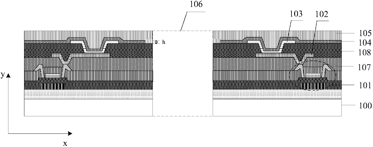
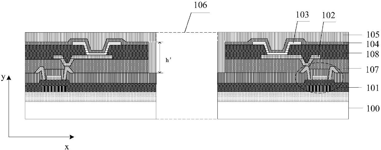
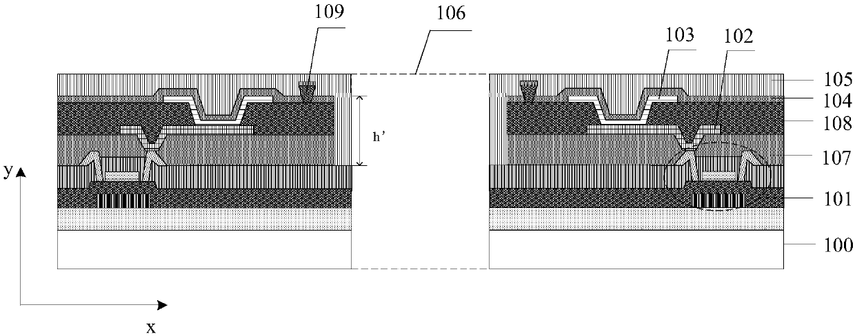
The invention relates to a display panel, a display device and a manufacturing method. The display panel, the display device and the manufacturing method are used for setting problems of area restriction of an effective displaying area and incapability of preparing a full screen caused by a manner of arranging a mounting hole in a non-displaying area of a display panel. The display panel comprisesa substrate, a TFT structure, an anode layer, a light emitting layer, a cathode layer and a packaging layer, wherein the TFT structure, the anode layer, the light emitting layer, the cathode layer and the packaging layer are successively arranged on the substrate. The displaying area is provided with the mounting hole for mounting a hardware structure. The mounting hole penetrates the structure and each film layer on the display panel. The edge of the mounting hole is provided with a packaging layer material with a preset thickness. The packaging layer material with the preset thickness at least covers the light emitting layer and the cathode layer which is adjacent with the edge of the mounting hole. The mounting hole is arranged in the displaying area, thereby realizing manufacturing ofthe full screen. Furthermore the packaging layer material with the preset thickness can perform a protecting function on the light emitting layer and the cathode layer, thereby preventing oxidation by external water and oxygen, and improving reliability at the position of the mounting hole.

Description

technical field [0001] The present invention relates to the field of display technology, in particular to a display panel, a display device and a manufacturing method. Background technique [0002] At present, flexible display devices usually adopt flexible OLED (Organic Light-Emitting Diode, organic light-emitting diode) devices, and flexible OLED devices are being widely used in smart terminal products such as mobile phones and tablet computers, because they are easy to customize the appearance More and more terminal manufacturers are applying it to full-screen and borderless products. Since full-screen and borderless products require a larger light-emitting area, in practical applications, it is usually necessary to use flexible organic light-emitting displays. Mounting holes are provided on the terminal device to reserve hardware installation positions such as the front camera, earpiece and start button on the terminal device. In the prior art, installation holes are ge...

Claims


Application Information

Patent Timeline
IPC IPC(8): H01L27/32H01L51/52
CPCH10K59/122H10K59/873Y02E10/549Y02P70/50H10K59/1201H10K59/00H10K50/844H10K77/10
Inventor 孙韬张嵩王涛
Owner BOE TECH GRP CO LTD
Learn More