Image reading device and semiconductor device
An image reading device and image reading technology, which are applied in semiconductor devices, image communication, electric solid-state devices, etc., can solve the problem that power saving is not considered.
- Summary
- Abstract
- Description
- Claims
- Application Information
AI Technical Summary
Problems solved by technology
Method used
Image
Examples
no. 1 approach
[0050] 1-1. Structure of compound machine
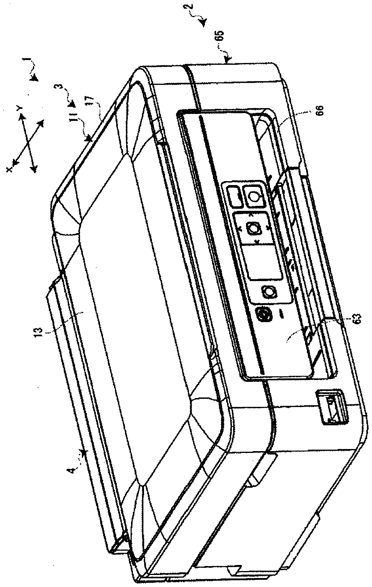
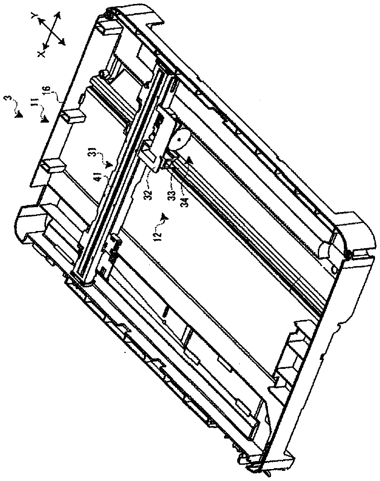
[0051] figure 1 It is a perspective view showing the appearance of the multi-function peripheral 1 . Such as figure 1 As shown, the multifunction peripheral 1 integrally includes a printer unit (image recording device) 2 as a main body, and a scanner unit (image reading device) 3 as an upper unit provided above the printer unit 2 . Additionally, in the following, the figure 1 In the description, the front-rear direction is referred to as the X-axis direction, and the left-right direction is referred to as the Y-axis direction.
[0052] On the other hand, if figure 1 As shown, the printer unit 2 is provided with: a conveyance unit (not shown) that conveys a single recording medium (printing paper or cut sheet) along the conveyance path; The printing part (not shown) that implements printing process on the recording medium; the operation part 63 of the panel form that is arranged on the front surface; ); the device housing 65 cov...
no. 2 approach
[0137]Hereinafter, with respect to the multifunction peripheral 1 of the second embodiment, the same reference numerals are assigned to the same constituent elements as those of the first embodiment, and overlapping descriptions with the first embodiment are omitted, and the differences from the first embodiment are mainly described. .
[0138] Since the structure of the compound machine 1 of the second embodiment is different from that of the first embodiment ( Figure 1 ~ Figure 4 ) are the same, so illustration and description thereof are omitted. Furthermore, since the functional block diagram of the scanner unit (image reading device) 3 in the second embodiment is different from that in the first embodiment ( Figure 5 ) are the same, so illustration and description thereof are omitted. In addition, since the functional block diagram of the image reading chip 415 in the second embodiment is different from that in the first embodiment ( Figure 6 ) are the same, so illu...
no. 3 approach
[0163] Hereinafter, with respect to the multifunction peripheral 1 of the third embodiment, the same reference numerals are attached to the same constituent elements as those of the first embodiment or the second embodiment, and descriptions that overlap with those of the first embodiment or the second embodiment are omitted. The content different from the first embodiment or the second embodiment will be described.
[0164] Since the structure of the compound machine 1 of the third embodiment is different from that of the first embodiment ( Figure 1 ~ Figure 4 ) are the same, so the illustration and description are omitted. Furthermore, since the functional block diagram of the scanner unit (image reading device) 3 in the third embodiment is different from that in the first embodiment ( Figure 5 ) are the same, so illustration and description thereof are omitted.
[0165] Figure 15 It is a functional block diagram of the image reading chip 415 in the third embodiment. ...
PUM
 Abstract
Description
Claims
Application Information
 - R&D
- Intellectual Property
- Life Sciences
- Materials
- Tech Scout
- Unparalleled Data Quality
- Higher Quality Content
- 60% Fewer Hallucinations
Browse by: Latest US Patents, China's latest patents, Technical Efficacy Thesaurus, Application Domain, Technology Topic, Popular Technical Reports.
© 2025 PatSnap. All rights reserved.Legal|Privacy policy|Modern Slavery Act Transparency Statement|Sitemap|About US| Contact US: help@patsnap.com


