Method for reducing photoelectrochemistry water decomposition starting potential of Ni/n-Si photo-anode
A technology of photoelectrochemistry and photoanode, which is applied in the field of photoelectrochemistry, can solve disadvantages and other problems, achieve the effect of reducing operation, low cost, and releasing the pinning effect of Fermi level
- Summary
- Abstract
- Description
- Claims
- Application Information
AI Technical Summary
Problems solved by technology
Method used
Image
Examples
Embodiment 1
[0025] The p-doped n-type single crystal Si sheet with a resistivity of 0.8-1Ω·cm was first soaked in H 2 SO 4 :H 2 o 2 Wash in a solution with a volume ratio of 3:1 for 10 minutes, then wash in H 2 O:HCl:H 2 o 2 Soak in a solution with a volume ratio of 5:1:1 at 75°C for 10 minutes for cleaning. Soak the cleaned sample in 4% dilute HF solution for 10 seconds to remove the surface oxide layer. Put the silicon wafer with the surface oxide layer removed immediately into the electron beam evaporation chamber, keep the chamber temperature at 50°C and the vacuum degree at 2×10 -4 Pa. by A deposition rate of about 20nm Ni thin film was deposited by electron beam evaporation on a silicon wafer to obtain a Ni / n-Si photoanode.
Embodiment 2
[0027] The Ni / n-Si photoanode prepared in Example 1 is put into a rapid heat treatment furnace, and the high-purity N 2 Under the atmosphere, rapid heat treatment is carried out at 450°C for 30 seconds, and the heating rate is 30°C / s. The heat treatment time of 30 seconds does not include the time spent in the heating process. A Ni / n-Si photoanode after rapid heat treatment was obtained.
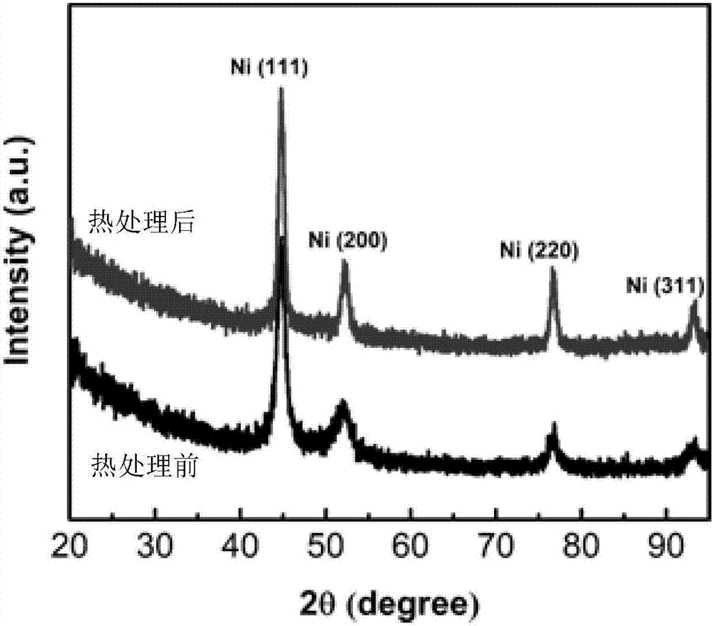
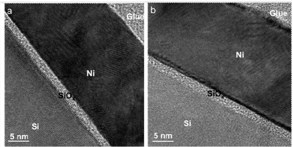
[0028] By comparing the XRD patterns and cross-sectional TEM images of Ni / n-Si photoanode before and after heat treatment, we can observe the phase and structure changes of Ni / n-Si photoanode before and after heat treatment. figure 1 It is the XRD pattern of Ni / n-Si before and after heat treatment. By comparison, we can find that the diffraction peak of Ni after heat treatment becomes sharper, and the half-peak width becomes narrower, indicating that the crystallinity of Ni after heat treatment is improved.
[0029] figure 2 (a) and (b) are the cross-sectional TEM images of the Ni / n-Si p...
Embodiment 3
[0032] The Ni / n-Si photoanode prepared in Example 1 is put into a rapid heat treatment furnace, and the high-purity N 2 Under atmosphere, rapid heat treatment is carried out at 550° C. for 30 seconds, and the heating rate is 30° C. / s. The heat treatment time of 30 seconds does not include the time spent in the heating process. A Ni / n-Si photoanode after rapid heat treatment was obtained.
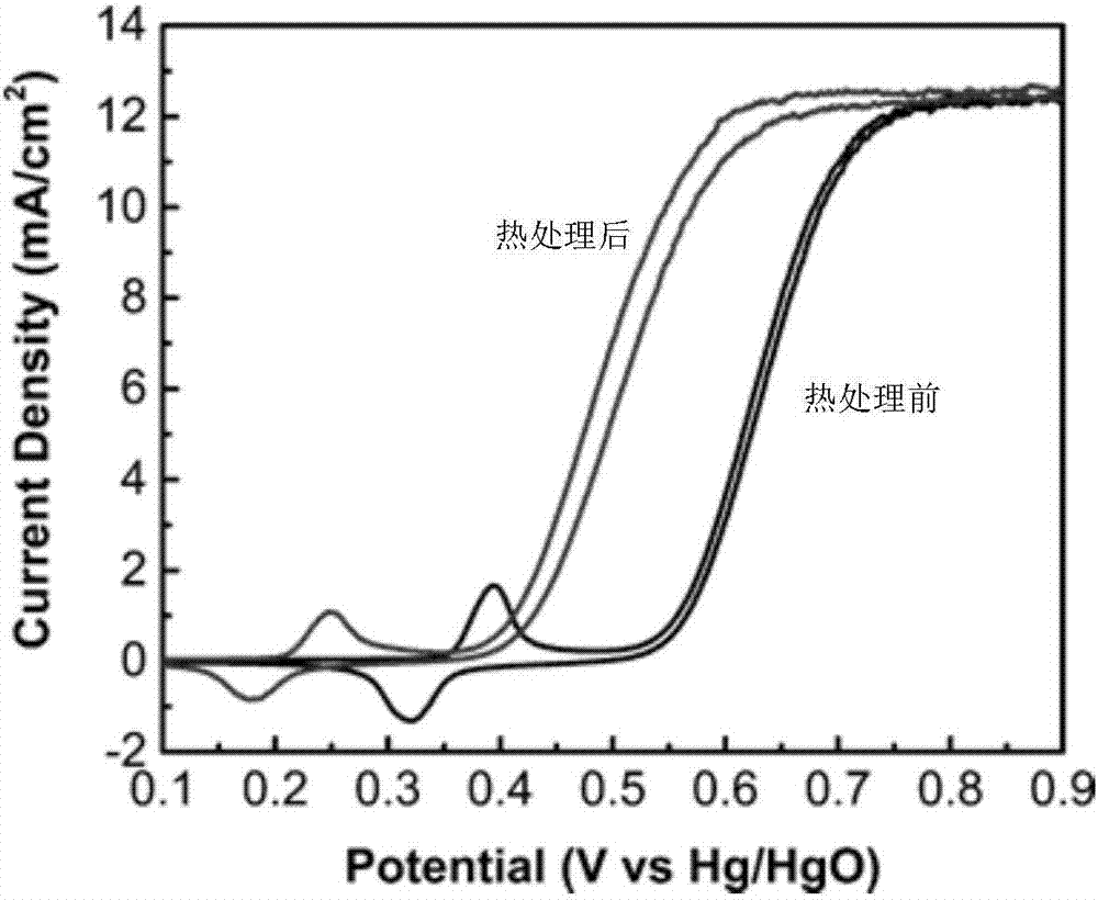
[0033] The C-V curves of Ni / n-Si photoanode before and after heat treatment are as follows Figure 4 As shown, we can find that the on-potential of the Ni / n-Si photoanode shifted negatively by 100mV after heat treatment.
PUM
 Abstract
Description
Claims
Application Information
 - Generate Ideas
- Intellectual Property
- Life Sciences
- Materials
- Tech Scout
- Unparalleled Data Quality
- Higher Quality Content
- 60% Fewer Hallucinations
Browse by: Latest US Patents, China's latest patents, Technical Efficacy Thesaurus, Application Domain, Technology Topic, Popular Technical Reports.
© 2025 PatSnap. All rights reserved.Legal|Privacy policy|Modern Slavery Act Transparency Statement|Sitemap|About US| Contact US: help@patsnap.com


