Semiconductor structure, self-supporting gallium nitride layer and preparation methods thereof

A gallium nitride layer and semiconductor technology, applied in semiconductor/solid-state device manufacturing, electrical components, circuits, etc., can solve problems such as poor universality, low yield, increased process steps and process complexity, etc., to improve growth quality , the effect of reducing stress

Active Publication Date: 2017-11-03
镓特半导体科技(上海)有限公司
View PDF5 Cites 0 Cited by
  • Summary
  • Abstract
  • Description
  • Claims
  • Application Information

AI Technical Summary

Problems solved by technology

Among them, laser lift-off technology is often used to separate gallium nitride grown on sapphire substrates. However, laser lift-off has high requirements on the flatness of gallium nitride crystals, and it is not easy to lift off larger-sized gallium nitride crystals; self-lift-off technology The stress generated by the thermal mismatch acts on the specific connection between the epitaxial GaN crystal and the heterogeneous substrate to make the epitaxial layer and the template fracture and separate. However, the thermal stress generated in the existing self-stripping process often causes the nitride The gallium epitaxial layer is broken, or the epitaxial layer cannot be peeled off. The self-stripping technology has high requirements for the growth process of the gallium nitride crystal, the design and production of the patterned substrate, and the yield of a complete gallium nitride crystal obtained by self-stripping is low; Mechanical stripping is the use of mechanical grinding to remove foreign substrates. However, mechanical stripping is suitable for low hardness and fragile foreign substrates; chemical etching stripping uses chemical agents that can remove foreign substrates and are not easy to corrode gallium nitride. To remove the foreign substrate on the back, chemical stripping requires the thermal stability of the foreign substrate to be good and easy to corrode
It can be seen from the above that the laser lift-off process, the mechanical lift-off process and the chemical etching lift-off process all need to perform an additional lift-off process after the gallium nitride growth process is completed, which increases the process steps and process complexity, thereby increasing the cost. At the same time, the laser lift-off process, mechanical stripping process, and chemical etching stripping process all have strict requirements on heterogeneous substrates, and their universality is poor; although the existing self-stripping process can realize self-striping of heterogeneous substrates and gallium nitride, the stripping The quality of gallium nitride will be affected during the process, and the yield rate is low

Method used


Image

  • Semiconductor structure, self-supporting gallium nitride layer and preparation methods thereof
  • Semiconductor structure, self-supporting gallium nitride layer and preparation methods thereof
  • Semiconductor structure, self-supporting gallium nitride layer and preparation methods thereof

Examples


Embodiment 1

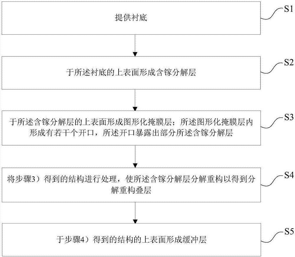
[0071] see figure 1 , the invention provides a method for preparing a semiconductor structure, the method for preparing a semiconductor structure includes the following steps:

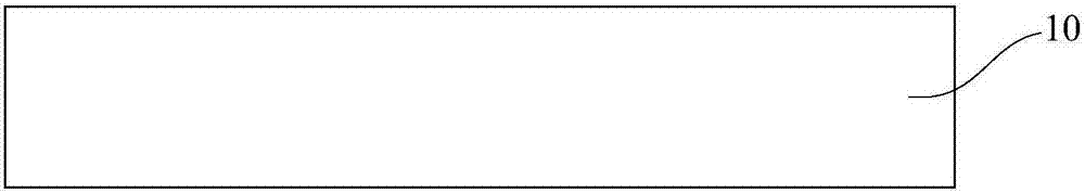
[0072] 1) Provide the substrate;

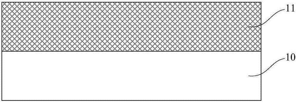
[0073] 2) forming a decomposed layer containing gallium on the upper surface of the substrate;

[0074] 3) forming a patterned mask layer on the upper surface of the gallium-containing decomposition layer; several openings are formed in the patterned mask layer, and the openings expose part of the gallium-containing decomposition layer;

[0075] 4) Process the structure obtained in step 3) to decompose and reconstruct the gallium-containing decomposed layer to obtain a decomposed and reconstructed stack, wherein the decomposed and reconstructed stack includes a reconstructed decomposed layer with several holes formed inside and a gallium nitride seed layer located on the upper surface of the reconstitution decomposition layer exposed by the opening;

[0076] 5) For...

Embodiment 2

[0119] Please combine Figure 1 to Figure 9 refer to Figure 10 to Figure 11 , the present invention also provides a method for preparing a semiconductor structure. The method for preparing a semiconductor structure described in this embodiment is substantially the same as the method described in Embodiment 1. The difference between the two is that the semiconductor structure of this embodiment Compared with the preparation method described in Example 1, a method for forming nitrogen on the upper surface of the substrate 10 is added between step 1) and step 2) of the preparation method described in Example 1. The step of forming the aluminum nitride layer 15, the aluminum nitride layer 15 is located between the substrate 10 and the gallium-containing decomposed layer 11; that is, the aluminum nitride layer 15 is first formed on the upper surface of the substrate 10 , and then form the gallium-containing decomposed layer 11 on the upper surface of the aluminum nitride layer 15...

Embodiment 3

[0125] Please combine Figure 10 and Figure 11 refer to Figure 12 to Figure 13 , the present invention also provides a method for preparing a semiconductor structure. The method for preparing a semiconductor structure described in this embodiment is substantially the same as the method described in Embodiment 2. The difference between the two is that the semiconductor structure of this embodiment Compared with the preparation method described in Example 2, the preparation method described in Example 2 also includes forming on the upper surface of the gallium-containing decomposition layer 11 between step 2) and step 3). The step of decomposing the barrier layer 16, the decomposing barrier layer 16 is located between the gallium-containing decomposing layer 11 and the patterned mask layer 12; barrier layer 16 , and then form the patterned mask layer 12 on the upper surface of the decomposition barrier layer 16 .

[0126] As an example, the decomposition barrier layer 16 ca...


PUM

PropertyMeasurementUnit
temperatureaaaaaaaaaa
thicknessaaaaaaaaaa
thicknessaaaaaaaaaa

Abstract

The invention provides a semiconductor structure, a self-supporting gallium nitride layer and preparation methods thereof. The preparation method of the semiconductor structure comprises the following steps: (1) providing a substrate; (2) forming a gallium-containing decomposed layer on the upper surface of the substrate; (3) forming a graphical mask layer on the upper surface of the structure obtained in the step (2); (4) processing the structure obtained in the step (3), so that the gallium-containing decomposed layer is decomposed and reconstructed so as to obtain a decomposed and reconstructed laminate; and (5) forming a buffer layer on the upper surface of the structure obtained in the step (4). When the semiconductor structure prepared by the preparation method of the semiconductor structure in the invention is used for growing gallium nitride, gallium nitride crystal seed layers in the decomposed and reconstructed laminate can be used for providing crystal seeds for subsequent gallium nitride growth, and holes inside the decomposed and reconstructed laminate are beneficial for automatic peeling for the subsequently grown gallium nitride and also can be used for reducing the stress among subsequently grown gallium nitride crystal lattices, so that the growth quality of gallium nitride can be improved.

Description

technical field [0001] The invention belongs to the technical field of semiconductors, and in particular relates to a semiconductor structure, a self-supporting gallium nitride layer and a preparation method thereof. Background technique [0002] The third-generation semiconductor materials are also called wide-bandgap semiconductors because their energy bandgap is generally greater than 3.0 electron volts. Compared with traditional silicon-based and gallium arsenide-based semiconductor materials, wide-bandgap semiconductors (such as silicon carbide, gallium nitride, aluminum nitride, and indium nitride, etc.) have unique bandgap ranges, excellent optical and electrical properties The properties and excellent material properties can meet the working requirements of high-power, high-temperature, high-frequency and high-speed semiconductor devices, and have a wide range of applications in the automotive and aviation industries, medical care, communications, military, general l...

Claims


Application Information

Patent Timeline
Patent Type & Authority Applications(China)
IPC IPC(8): H01L21/02H01L21/324H01L21/78
CPCH01L21/02458H01L21/02513H01L21/02658H01L21/02694H01L21/3245H01L21/7813
Inventor 罗晓菊王颖慧
Owner 镓特半导体科技(上海)有限公司
Why Eureka
Try Eureka