Bistable liquid crystal device with optical writing or optical erasing function and preparation method thereof
A bistable liquid crystal and optical writing technology, which is applied in the fields of instruments, optics, nonlinear optics, etc., can solve problems such as difficult control and complicated process, and achieve the effects of simple processing, simple synthesis, and large-area production
- Summary
- Abstract
- Description
- Claims
- Application Information
AI Technical Summary
Problems solved by technology
Method used
Image
Examples
Embodiment 1
[0048] Example 1: Electrical writing, optical erasing
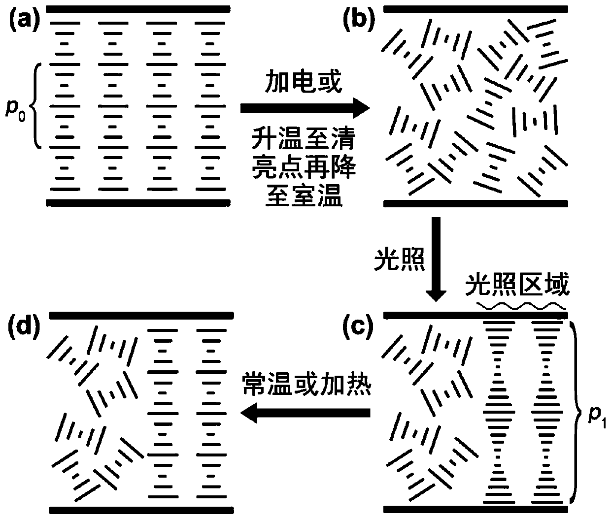
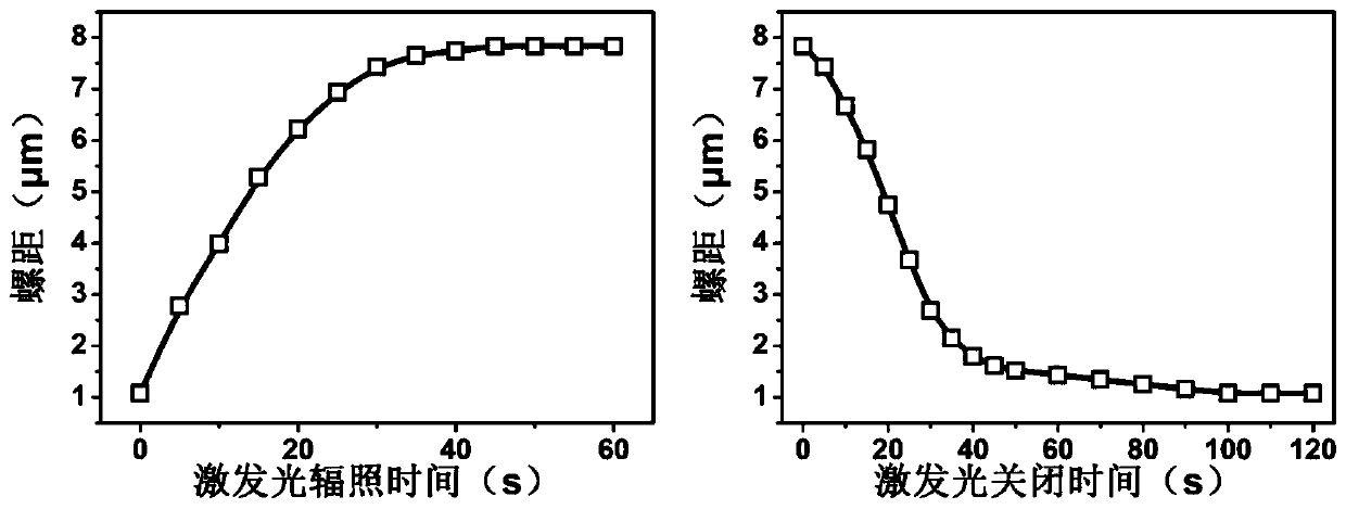
[0049] The composite system of chiral helicene compound (right-handed) / R811 (right-handed) / nematic liquid crystal SLC1717 is blended according to the ratio of 1.00 / 5.30 / 93.70 to prepare a photoresponsive cholesteric liquid crystal composite system. Such as image 3 As shown, under excitation light (365nm, 10.0mW / cm 2 ) irradiation, the pitch of the photoresponsive cholesteric liquid crystal changes from p 0 = 1.1 μm becomes p 1 =7.8μm; when the excitation light is turned off, the pitch starts from p 1 = 7.8 μm reverts to p 0 = 1.1 μm. First, the liquid crystal composite system is poured into a liquid crystal cell with a cell thickness of 20 μm. The liquid crystal is in a planar texture, showing a transparent selective reflection state, and the visible light transmittance is about 95% ( Pic 4-1 ). Apply an electric field to the circular area where information needs to be written, and the arrangement of the liquid c...
Embodiment 2
[0052] Example 2: Electrical writing, optical erasing
[0053] Chiral helicene compound (left-handed) / S811(left-handed) / nanoparticle NaYF 4 : The compound system of Yb, Er / nematic liquid crystal E7 is blended according to the ratio of 1.60 / 4.80 / 0.90 / 92.70 to prepare a photoresponsive cholesteric liquid crystal compound system. Under excitation light (975nm, 200.0W / cm 2 ) irradiation, nanoparticles NaYF 4 :Yb,Er will emit ultraviolet light excited in situ, and the pitch of the photoresponsive cholesteric liquid crystal changes from p 0 =0.7μm becomes p 1 =3.7μm; when the excitation light is turned off, the pitch starts from p 1 = 3.7 μm reverts to p 0 = 0.7 μm. First, the liquid crystal composite system is poured into a liquid crystal cell with a cell thickness of 70 μm. The liquid crystal is in a plane texture, showing a transparent selective reflection state, and the visible light transmittance is about 94%. When an electric field is applied to the circular area where ...
Embodiment 3
[0056] Example 3: Optical writing, electrical erasing
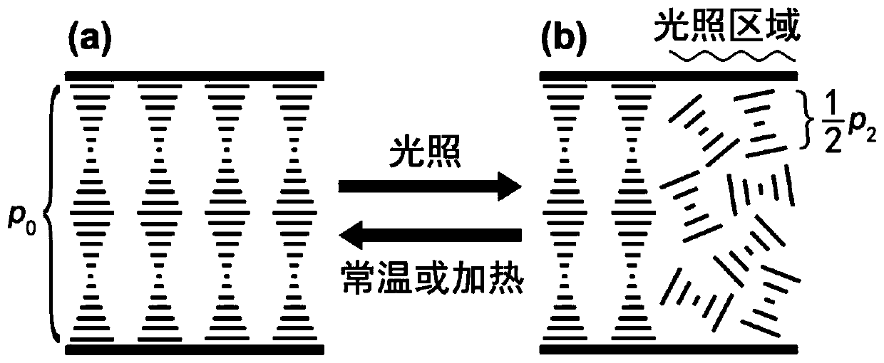
[0057] The composite system of chiral helicene compound (right-handed) / R811 (right-handed) / nematic liquid crystal SLC1717 is blended according to the ratio of 1.40 / 5.10 / 93.50 to prepare a photoresponsive cholesteric liquid crystal composite system. Under excitation light (400nm, 30.0mW / cm 2 ) irradiation, the pitch of the photoresponsive cholesteric liquid crystal changes from p 0 = 1.0 μm becomes p 1 =9.4μm; when the excitation light is turned off, the pitch starts from p 1 = 9.4 μm reverts to p 0 = 1.0 μm. First, the liquid crystal composite system is poured into a liquid crystal cell with a cell thickness of 2 μm, and then an electric field is applied to the liquid crystal cell to make the arrangement of the liquid crystal molecules into a focal conic state, showing a light scattering state, and the transmittance is about 12% ( Figure 6-1 ). Then using excitation light (400nm, 30.0mW / cm 2 ) to irradiate the tri...
PUM
| Property | Measurement | Unit |
|---|---|---|
| thickness | aaaaa | aaaaa |
Abstract
Description
Claims
Application Information
 - R&D
- Intellectual Property
- Life Sciences
- Materials
- Tech Scout
- Unparalleled Data Quality
- Higher Quality Content
- 60% Fewer Hallucinations
Browse by: Latest US Patents, China's latest patents, Technical Efficacy Thesaurus, Application Domain, Technology Topic, Popular Technical Reports.
© 2025 PatSnap. All rights reserved.Legal|Privacy policy|Modern Slavery Act Transparency Statement|Sitemap|About US| Contact US: help@patsnap.com


