Eureka AIR delivers breakthrough ideas for toughest innovation challenges, trusted by R&D personnel around the world.

UV light emitting diode with double doped multi-quantum well structure

A multi-quantum well structure, light-emitting diode technology, applied in electrical components, circuits, semiconductor devices, etc., can solve the problems of UV-LED luminous efficiency decline, uneven distribution of carriers, electron overflow, etc., to suppress red shift , Improve radiation recombination efficiency, eliminate the effect of energy band tilt

Active Publication Date: 2017-10-10
SOUTHEAST UNIV
View PDF21 Cites 16 Cited by
  • Summary
  • Abstract
  • Description
  • Claims
  • Application Information

AI Technical Summary

Problems solved by technology

However, reducing the thickness of the well layer in the quantum well will impose extremely high requirements on the steepness of the heterojunction interface, and reducing the depth of the quantum well will increase the uneven distribution of carriers, specifically manifested as a large number of electrons will accumulate in the In the last quantum well of the multi-quantum well structure, it is easy to cause electron overflow
Therefore, the existing technology cannot effectively solve the problem of the decrease of UV-LED luminous efficiency due to the polarization electric field in polar devices.

Method used


Image

  • UV light emitting diode with double doped multi-quantum well structure
  • UV light emitting diode with double doped multi-quantum well structure
  • UV light emitting diode with double doped multi-quantum well structure

Examples


Embodiment Construction

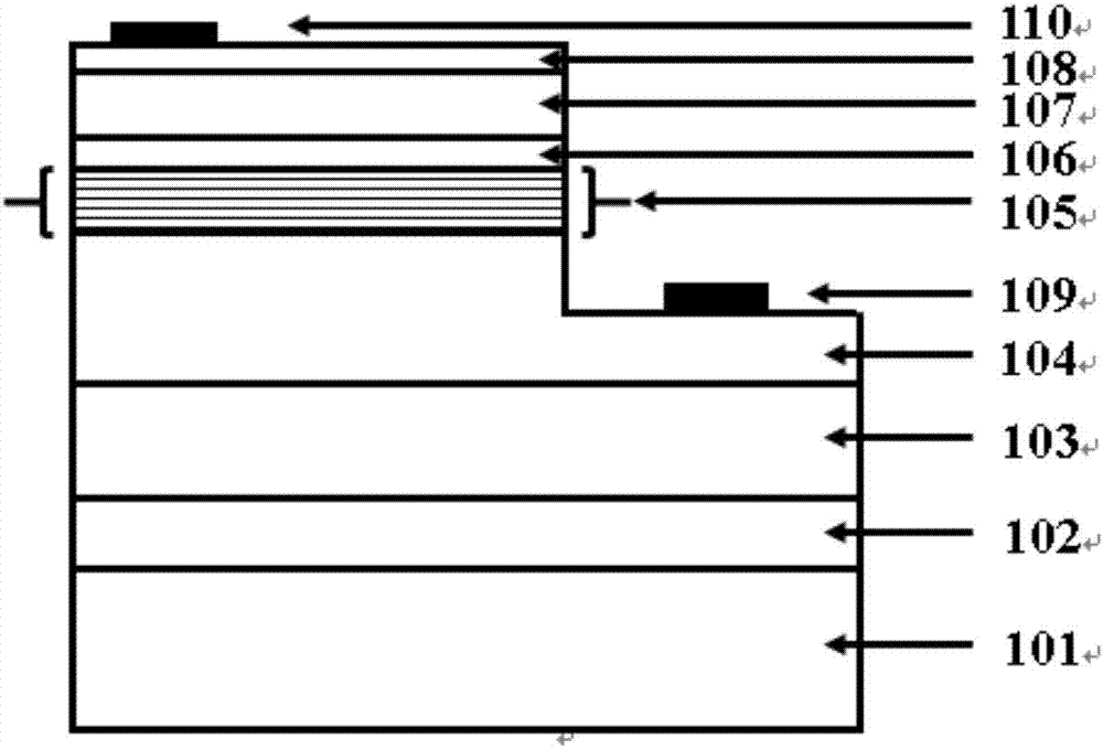
[0017] Such as figure 1 As shown, an ultraviolet light-emitting diode with a double-doped multiple quantum well structure includes: a polar c-plane sapphire substrate 101, an AlN intermediate layer 102, a non-doped AlGaN buffer layer 103, and an n-type AlGaN layer 104, doubly doped Al x Ga 1-x N / Al y Ga 1-y N multiple quantum well active region 105, Al z Ga 1-z N electron blocking layer 106, where z>y>x, p-type AlGaN layer 107 and transparent conductive layer 108, n-type ohmic electrode 109 and p-type ohmic electrode 110 respectively provided on the n-type AlGaN layer and transparent conductive layer.

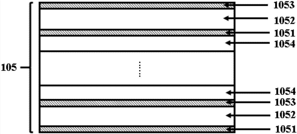
[0018] figure 2 A schematic diagram of the enlarged cross-sectional structure of the double-doped multiple quantum well structure part 105 of the UV-LED with a double-doped multiple quantum well structure provided by the present invention, characterized in that: the double-doped multiple quantum well 105 is from bottom to bottom which in turn consists of n-type doped A...


PUM


Abstract

The invention discloses a UV light emitting diode with double doped multi-quantum well structure, which comprises the following elements arranged from the bottom to the top in a successive manner: an AlN intermediate layer, an un-doped AlGaN buffer layer, an n-type AlGaN layer and a double doped AlxGa1-xN / AlyGa1-yN multi-quantum well passive area, an AlzGa1-zN electron blocking layer with z greater than y and y greater than x, a p-type AIGaN layer and a transparent conductive layer. On the n-type AlGaN layer and the transparent conductive layer are provided with an n-type Ohmic electrode and a p-type Ohmic electrode respectively. The beneficial effects of the present invention are as follows: a compensation electric field in opposite polarized electric field direction can be formed, which, on one hand, reduces or even eliminates the energy band inclination of the quantum well, increases the effective height of the quantum well barrier layer, increases the uniform distribution of carriers especially in the multi-quantum well structure and, on the other hand, increases the overlapping of the electrons in the quantum well with the wave function in space and increases the radiation composite efficiency of the electrons and the electron holes, therefore raising the UV-LED luminance efficiency substantially.

Description

technical field [0001] The invention relates to the technical field of semiconductor optoelectronic materials and device manufacturing, in particular to an ultraviolet light-emitting diode with a double-doped multi-quantum well structure. Background technique [0002] Due to its high photon energy and strong penetrating ability, ultraviolet light is widely used in fields such as sterilization, water and air purification, solid-state lighting, detection of biochemical harmful substances, high-density storage, and military communications. [0003] AlGaN material is the core material for making UV-LED. First of all, Al x Ga 1-x N material is a wide bandgap direct bandgap semiconductor material. By adjusting the Al composition in the ternary compound AlGaN, the AlGaN bandgap energy can be continuously changed between 3.4 and 6.2eV, thereby obtaining ultraviolet light with a wavelength range from 210 to 365nm. Light. Second, Al x Ga 1-x N is a compound with strong ionic bon...

Claims


Application Information

Patent Timeline
Patent Type & Authority Applications(China)
IPC IPC(8): H01L33/06H01L33/12H01L33/24H01L33/32
CPCH01L33/06H01L33/12H01L33/24H01L33/325
Inventor 张雄范艾杰吴自力崔一平
Owner SOUTHEAST UNIV
Why Eureka
Eureka Blog
Learn More