Optical fingerprint sensing packaging structure
A packaging structure, optical technology, applied in the direction of acquiring/arranging fingerprints/palmprints, character and pattern recognition, instruments, etc., can solve the problems of complex structural design, large volume of optical mechanism, reduction, etc., to achieve volume reduction and thin thickness , space-saving effect
- Summary
- Abstract
- Description
- Claims
- Application Information
AI Technical Summary
Problems solved by technology
Method used
Image
Examples
Embodiment Construction
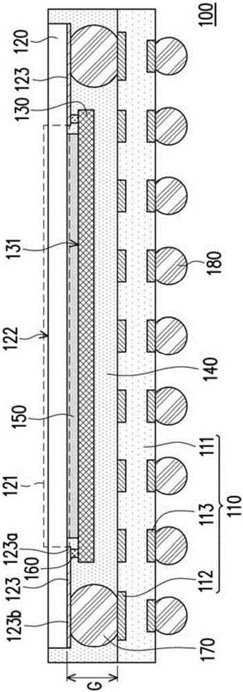
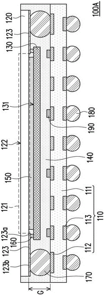
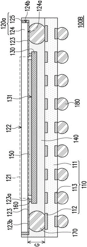
[0050] figure 1 is a schematic cross-sectional view of the optical fingerprint sensing package structure of the first embodiment of the present invention. Please refer to figure 1 , in this embodiment, the optical fingerprint sensing package structure 100 includes a circuit carrier 110 , an optical element 120 , a fingerprint sensing chip 130 and a packaging compound 140 . The circuit carrier 110 can be a rigid circuit board or a flexible circuit board, which includes a dielectric layer 111 , a first patterned circuit layer 112 and a second patterned circuit layer 113 . The first patterned wiring layer 112 and the second patterned wiring layer 113 are respectively located on opposite sides of the dielectric layer 111, and can selectively pass through the multilayer metal layers or conductive vias (plated) disposed in the dielectric layer 111. through hole / via) electrical connection. The optical element 120 is disposed above the circuit carrier 110 and is electrically connec...
PUM
 Abstract
Description
Claims
Application Information
 - R&D Engineer
- R&D Manager
- IP Professional
- Industry Leading Data Capabilities
- Powerful AI technology
- Patent DNA Extraction
Browse by: Latest US Patents, China's latest patents, Technical Efficacy Thesaurus, Application Domain, Technology Topic, Popular Technical Reports.
© 2024 PatSnap. All rights reserved.Legal|Privacy policy|Modern Slavery Act Transparency Statement|Sitemap|About US| Contact US: help@patsnap.com


