High-density subminiature thick-film chip resistor and manufacturing method therefor

A chip resistor and manufacturing method technology, applied in resistor manufacturing, thick film resistors, resistors and other directions, can solve the problems of low utilization rate of production materials, environmental impact of waste, low manufacturing accuracy, etc., to achieve low manufacturing costs and meet application requirements Requirement, the effect of simple structure

Inactive Publication Date: 2017-09-08
丽智电子(南通)有限公司
View PDF6 Cites 2 Cited by
  • Summary
  • Abstract
  • Description
  • Claims
  • Application Information

AI Technical Summary

Problems solved by technology

[0004] The purpose of the present invention is to overcome the problems of existing high-density ultra-small thick-film chip resistors, low manufacturing precision, low utilization rate of production materials, high production cost, and the impact of waste on the environment

Method used


Image

  • High-density subminiature thick-film chip resistor and manufacturing method therefor
  • High-density subminiature thick-film chip resistor and manufacturing method therefor
  • High-density subminiature thick-film chip resistor and manufacturing method therefor

Examples


Embodiment Construction

[0048] The present invention will be further described below in conjunction with the accompanying drawings.

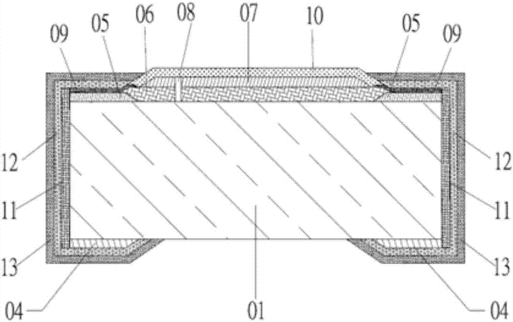
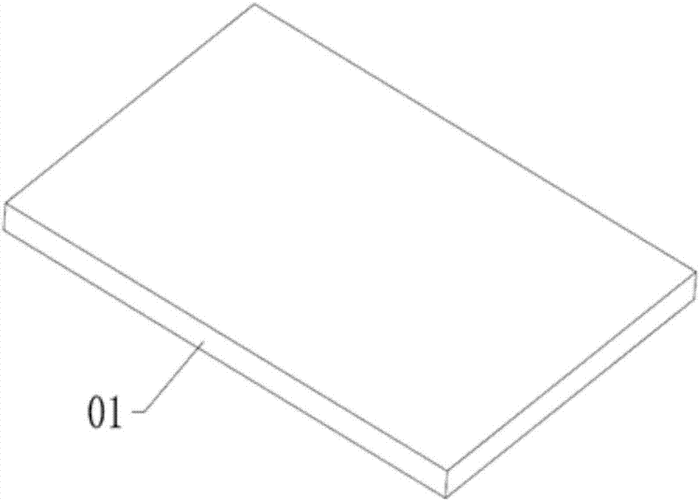
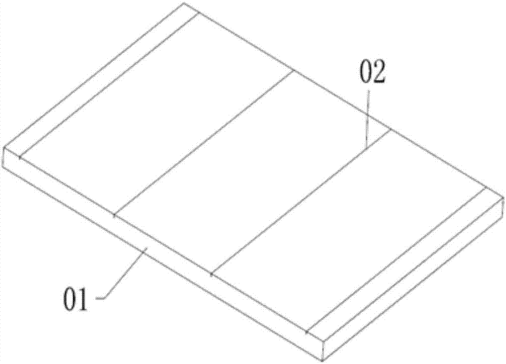
[0049] Such as figure 1 As shown, the high-density ultra-small thick film chip resistor of the present invention includes a ceramic substrate 01, the two long sides of the back of the ceramic substrate 01 are provided with folding lines 02, and the front two short sides of the ceramic substrate 01 are provided with There are folded grain lines 03, the folded grain lines 02 and the folded grain lines 03 are vertically arranged in the space, the back electrode 04 is printed on the back of the ceramic substrate 01, and the folded grain lines 03 are printed on the front of the ceramic substrate 01. The inner side is symmetrically printed with a first front electrode 05, and a resistance body 06 is printed between the two first front electrodes 05. The upper surface of the resistance body 06 is provided with a first protective layer 07, and the resistance body 06 and A rad...


PUM


Abstract

The invention discloses a high-density subminiature thick-film chip resistor and a manufacturing method therefor. The resistor comprises a ceramic substrate; folding strip lines are arranged on the two long side edges of the back surface of the ceramic substrate; folding grain lines are arranged on the two short side edges of the front surface of the ceramic substrate; the folding strip lines and the folding grain lines are arranged perpendicularly in a space; a back surface electrode is printed on the back surface of the ceramic substrate; first front surface electrodes are symmetrically printed on the inner sides of the folding grain lines on the front surface of the ceramic substrate; a resistor body is printed between the two first front surface electrodes; a first protection layer is arranged on the upper surface of the resistor body; a radium tangent line is arranged on the resistor body and the first protection layer; second front surface electrodes are arranged on the upper surfaces of the two first front surface electrodes; a second protection layer is arranged on the upper surface of the radium tangent line; and side surface electrodes are arranged on the two side surfaces of the ceramic substrate on the two sides of the first front surface electrodes. The high-density subminiature thick-film chip resistor is simple in structure, convenient to use, high in density, subminiature in size, and relatively low in manufacturing cost, and has high application prospect.

Description

technical field [0001] The invention relates to the technical field of electronic components, in particular to a high-density ultra-small thick-film chip resistor and a manufacturing method thereof. Background technique [0002] With the advancement of science and technology, the development of the times and the continuous improvement of people's requirements for various electronic products, in recent years, consumers' continuous demand for ultra-small, high-performance, multi-functional, portable and wearable electronic products has prompted various Class electronic products tend to develop rapidly in the direction of "light", "thin", "short" and "small", which makes high-density ultra-small thick film chip resistors (model 01005) popularized and applied. [0003] At present, the application of high-density ultra-small thick-film chip resistors is becoming more and more widespread, which brings challenges to equipment and processes, because high-density ultra-small thick-fi...

Claims


Application Information

Patent Timeline
Patent Type & Authority Applications(China)
IPC IPC(8): H01C7/00H01C1/142H01C17/065H01C17/28
CPCH01C1/142H01C7/003H01C17/065H01C17/281
Inventor 黄正信刘复强陈庆良魏效振
Owner 丽智电子(南通)有限公司
Why Eureka
Try Eureka