Method for reducing silicon-based optical waveguide sidewall roughness
A silicon-based optical waveguide and rough side wall technology, which is applied in the direction of optical waveguide light guide, light guide, optics, etc., can solve the problem of large side wall roughness of silicon-based optical waveguide, achieve the reduction of side wall roughness and maintain the shape and size, the effect of reducing roughness
- Summary
- Abstract
- Description
- Claims
- Application Information
AI Technical Summary
Problems solved by technology
Method used
Image

Examples
Embodiment 1
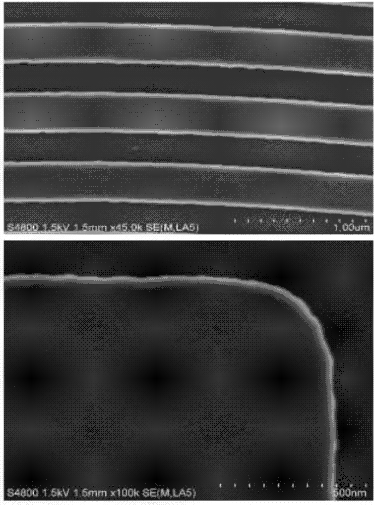
[0050] Providing a substrate; forming a silicon-based optical waveguide line on the substrate; hydrogen annealing the substrate containing the silicon-based optical waveguide line, the chamber pressure for the hydrogen annealing is 20 Torr, and the annealing temperature is 950°C, Among them, the heating rate is 2-5°C / s, the annealing time is: 10s, the annealing chamber is loaded with hydrogen as a protective gas, and the hydrogen flow rate is: 180L / min.
[0051] Under high-temperature annealing conditions, hydrogen will interact with the dangling bonds on the adjacent dimers on the surface of the silicon-based optical waveguide to promote the formation of silicon-hydrogen bonds. Due to the existence of the silicon-hydrogen bond, the silicon-hydrogen bond flow density vector tends to shift from a high-energy state to a low-energy state, which enhances the activity of silicon atoms on the surface of the waveguide and increases the atomic mobility, so as to better realize the smoothi...
Embodiment 2
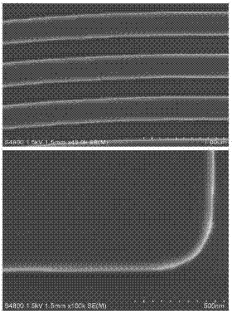
[0053] The difference between Embodiment 2 and Embodiment 1 is that the pressure of the hydrogen annealing chamber is increased from 20 Torr in Embodiment 1 to a standard atmospheric pressure.
[0054] Example 2:
[0055] Providing a substrate; forming a silicon-based optical waveguide line on the substrate; hydrogen annealing the substrate containing the silicon-based optical waveguide line, the chamber pressure of the hydrogen annealing is 1atm, and the annealing temperature is 950°C, Among them, the heating rate is 2-5°C / s, the annealing time is: 10s, the annealing chamber is loaded with hydrogen as a protective gas, and the hydrogen flow rate is: 180L / min.
[0056] Under high-temperature annealing conditions, hydrogen will interact with the dangling bonds on the adjacent dimers on the surface of the silicon-based optical waveguide to promote the formation of silicon-hydrogen bonds. Due to the existence of the silicon-hydrogen bond, the silicon-hydrogen bond flow density vector t...
Embodiment 3
[0059] The difference between Example 3 and Example 1 is that the hydrogen annealing temperature is adjusted from 950° C. in Example 1 to 600° C., the annealing time is adjusted from 10 s to 30 s in Example 1, and an etching gas is introduced.
[0060] Example 3:
[0061] Providing a substrate; forming a silicon-based optical waveguide line on the substrate; hydrogen annealing the substrate containing the silicon-based optical waveguide line, the chamber pressure of the hydrogen annealing is 20 Torr, and the annealing temperature is 600°C, Among them, the heating rate is 2-5°C / s, the annealing time is: 30s, the annealing chamber is loaded with hydrogen as a protective gas, the hydrogen flow is: 180L / min, the etching gas hydrogen chloride is introduced, and the flow of hydrogen chloride is 10 sccm.
[0062] The etching gas selected in the present invention is preferably hydrogen chloride, but is not limited to hydrogen chloride. The flow rate of the hydrogen chloride is 10-200 sccm, ...
PUM
 Abstract
Description
Claims
Application Information
 - Generate Ideas
- Intellectual Property
- Life Sciences
- Materials
- Tech Scout
- Unparalleled Data Quality
- Higher Quality Content
- 60% Fewer Hallucinations
Browse by: Latest US Patents, China's latest patents, Technical Efficacy Thesaurus, Application Domain, Technology Topic, Popular Technical Reports.
© 2025 PatSnap. All rights reserved.Legal|Privacy policy|Modern Slavery Act Transparency Statement|Sitemap|About US| Contact US: help@patsnap.com