Processing method for improving second generation high-temperature super-conducting strip interlayer binding force
A technology of high-temperature superconducting tape and interlayer bonding force, applied in the usage of superconducting elements, equipment for manufacturing conductive/semiconducting layers, superconducting devices, etc., can solve the problems affecting the robustness of processing technology, layer Poor bonding force between layers, low bonding force between layers, etc.
- Summary
- Abstract
- Description
- Claims
- Application Information
AI Technical Summary
Problems solved by technology
Method used
Image
Examples
Embodiment 1
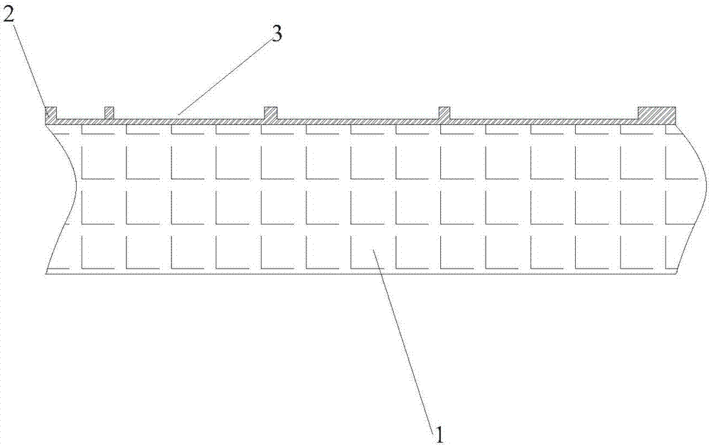
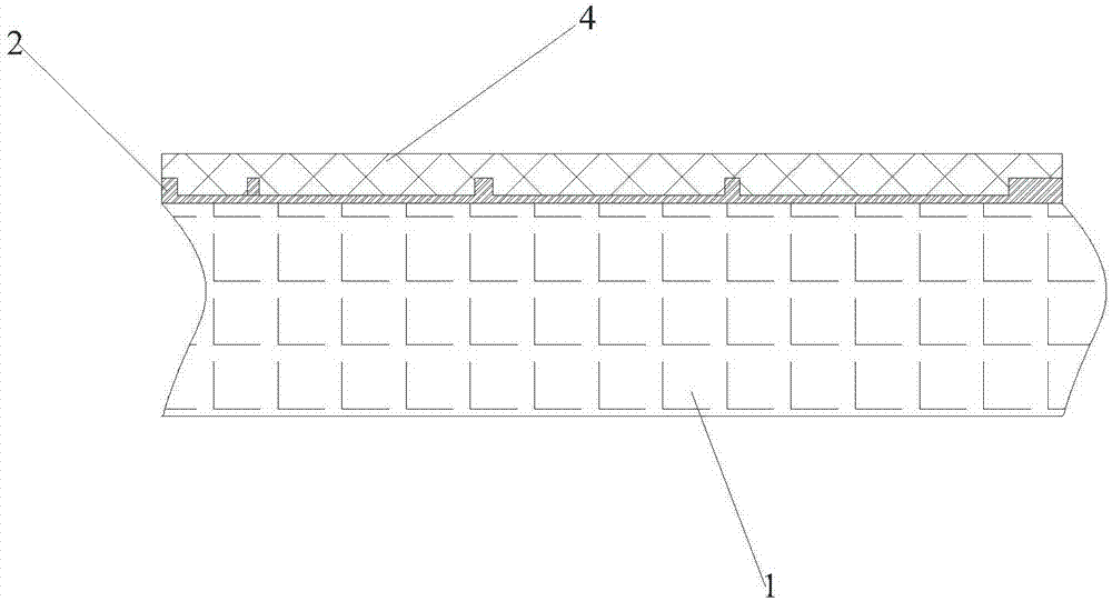
[0034] This embodiment relates to a preparation method for improving the interlayer bonding force of the second-generation high-temperature superconducting tape, and the method includes the following steps:
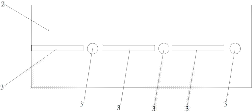
[0035] 1) Etching process: select the structure as CeO 2 / MgO / Y 2 o 3 / Al 2 o 3 / C276 Textured flexible tape, on CeO 2 The oxide layer is etched; the etching technology is laser etching, the laser can provide laser with a wavelength in the ultraviolet band, the diameter of the laser spot is less than 2 microns, the laser etching frequency is 10 Hz, and the moving speed of the laser spot is 20 mm / s; Optical microscope photographs of the eclipse area, such as Figure 5 shown;
[0036] 2) Superconducting thin film deposition process: Deposit a superconducting layer on the surface of the textured flexible strip obtained in step 1), the process of depositing the superconducting layer is physical vapor deposition technology, and the material of the superconducting layer i...
Embodiment 2
[0038] This embodiment relates to a preparation method for improving the interlayer bonding force of the second-generation high-temperature superconducting tape, and the method includes the following steps:
[0039] 1) Etching process: select the structure as LaMnO 3 / MgO / Y 2 o 3 / Al 2 o 3 / SS textured flexible tape, for LaMnO 3 The oxide layer is etched; the etching technology is laser etching;
[0040] 2) Superconducting film deposition process: Deposit a superconducting layer on the surface of the textured flexible strip obtained in step 1), the process of depositing the superconducting layer is chemical vapor deposition technology, and the material of the superconducting layer is Gd 0.5 Y 0.5 Ba 2 Cu 3 o 7, step 1) does not affect the optimized process parameters for depositing the superconducting layer, and the deposition process is the same as that of the substrate without surface etching. The performance test result shows that the critical delamination stress ...
Embodiment 3
[0042] This embodiment relates to a preparation method for improving the interlayer bonding force of the second-generation high-temperature superconducting tape, and the method includes the following steps:
[0043] 1) Etching process: select the structure as CeO 2 / YSZ / Y 2 o 3 / NiW textured flexible tape, on CeO 2 The oxide layer is etched; the etching technique is chemical etching;
[0044] 2) Superconducting film deposition process: Deposit a superconducting layer on the surface of the textured flexible strip obtained in step 1), the process of depositing the superconducting layer is chemical vapor deposition technology, and the material of the superconducting layer is Gd 0.5 Y 0.5 Ba 2 Cu 3 o 7 with a molar content of 5% BaZrO 3 The composite superconductor; step 1) does not affect the optimized process parameters for depositing the superconducting layer, and the deposition process is the same as that of the substrate without surface etching. The performance test ...
PUM
| Property | Measurement | Unit |
|---|---|---|
| diameter | aaaaa | aaaaa |
| thickness | aaaaa | aaaaa |
Abstract
Description
Claims
Application Information
 - R&D
- Intellectual Property
- Life Sciences
- Materials
- Tech Scout
- Unparalleled Data Quality
- Higher Quality Content
- 60% Fewer Hallucinations
Browse by: Latest US Patents, China's latest patents, Technical Efficacy Thesaurus, Application Domain, Technology Topic, Popular Technical Reports.
© 2025 PatSnap. All rights reserved.Legal|Privacy policy|Modern Slavery Act Transparency Statement|Sitemap|About US| Contact US: help@patsnap.com


