System and method for detecting surface defect of solar cell panel
A solar panel and defect detection technology, applied in the field of image processing, can solve the problems of not being able to adapt to the defect requirements of the production process, the difficulty of achieving consistent detection standards, and the difficulty of improving the efficiency of manual detection, etc., to achieve strong anti-interference ability and fast speed on site , The effect of improving the operation speed
- Summary
- Abstract
- Description
- Claims
- Application Information
AI Technical Summary
Problems solved by technology
Method used
Image


Examples
Embodiment 1
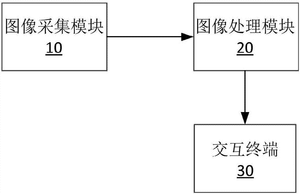
[0031] see figure 1 , is a schematic structural diagram of a solar panel surface defect detection system according to Embodiment 1 of the present invention, a solar panel surface defect detection system, including an image acquisition module 10, an image processing module 20 and an interactive terminal 30, wherein,
[0032] The image acquisition module 10 outputs the captured solar panel image to the image processing module 20 for image processing and solar panel surface defect analysis, and the output of the image processing module 20 is connected to the interactive terminal 30, The interactive terminal 30 receives the instruction and responds in real time and displays the type and location of the surface defect of the solar cell panel.
[0033] Through the solar panel surface defect detection system set up above, the front-end is composed of an image acquisition module 10 , a back-end image processing module 20 and an interactive terminal 30 . The front-end image acquisitio...
Embodiment 2
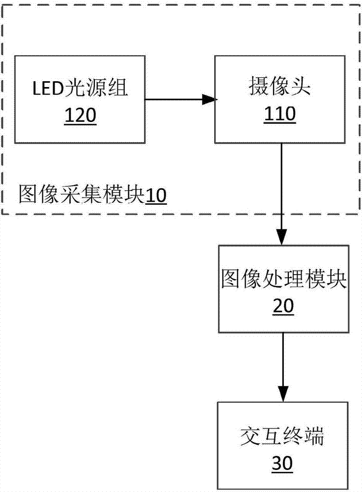
[0035] see figure 2 , which is a schematic structural diagram of a solar cell panel surface defect detection system according to an embodiment of the present invention.
[0036] The image acquisition module 10 includes a camera 110 and an LED light source group 120 , and the LED light source group 120 supplements light when the camera 110 collects images.
[0037] The above-mentioned camera 110 adopts a CCD type and is responsible for capturing raw image data and outputting analog video signals to the rear end. In this embodiment, a 5-megapixel industrial camera of the VCXG-53M model of the German Baumer Company is selected. The camera uses a GigE power supply: an external 12-24V or PoE (Power over Ethernet). The specific embodiment can also include XW0816 high-definition industrial lens. XW0816 is a 5-megapixel high-definition precision industrial lens that supports 8-16mm zoom. It is a high-resolution lens specially used in machine vision, medical imaging, biological detec...
Embodiment 3
[0039] see image 3 , which is a schematic structural diagram of a solar cell panel surface defect detection system according to an embodiment of the present invention.
[0040] The image processing module 20 includes a preprocessing unit 210, an image segmentation unit 220, and a pattern recognition unit 230. The three are connected in sequence to identify defects on the surface of the solar panel, and process and evaluate the type, size, color and depth of the defects. The pattern recognition unit 230 at least includes a color difference recognition subunit, a dirt recognition subunit and a defect recognition subunit.
[0041] The preprocessing unit 210 at least completes the median filtering and edge detection subunits, wherein,
[0042] Median filtering: Perform two-dimensional median filtering on the image. Its function is to remove noise and protect the edge of the image, which also belongs to image enhancement. The two-dimensional median filter can be expressed by th...
PUM
 Abstract
Description
Claims
Application Information
 - Generate Ideas
- Intellectual Property
- Life Sciences
- Materials
- Tech Scout
- Unparalleled Data Quality
- Higher Quality Content
- 60% Fewer Hallucinations
Browse by: Latest US Patents, China's latest patents, Technical Efficacy Thesaurus, Application Domain, Technology Topic, Popular Technical Reports.
© 2025 PatSnap. All rights reserved.Legal|Privacy policy|Modern Slavery Act Transparency Statement|Sitemap|About US| Contact US: help@patsnap.com