
Small-sized welding packaging high power simulation optical module

A technology for welding packaging and optical modules, which is applied in the direction of light guides, optics, and optical components, can solve problems such as increased difficulty of development projects, extended development cycles, and device compatibility that affect the operation reliability of final products, so as to save raw materials and space. The effect of stable linear range and small form factor

Inactive Publication Date: 2017-07-18
NO 34 RES INST OF CHINA ELECTRONICS TECH GRP +1
View PDF5 Cites 2 Cited by
  • Summary
  • Abstract
  • Description
  • Claims
  • Application Information

AI Technical Summary

Problems solved by technology

This increases the difficulty of related development projects, prolongs the development cycle, and makes related production passive, and also affects the operational reliability and device compatibility of final products.

Method used


Image

  • Small-sized welding packaging high power simulation optical module

Examples


Embodiment Construction

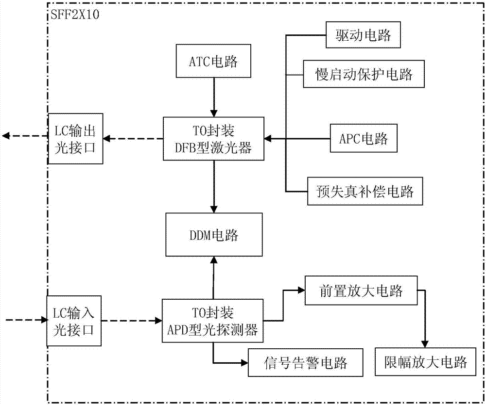
[0022] The implementation of the high-power analog optical module in this miniaturized solderable package is as an example figure 1As shown, the dotted arrows in the figure indicate the optical signal connection, and the solid line arrows indicate the electrical signal connection. The emitting optoelectronic device of the optical module in this example is a DFB analog laser. The core of the analog laser light source stripped of the redundant external circuit is placed in a TO package and coaxially packaged. The receiving optoelectronic device is an APD type photodetector, which is placed in another TO package. Inner coaxial package. The analog laser and photodetector are respectively connected to the LC-type output and input optical interfaces. The drive circuit and the slow start protection circuit are connected to the DFB laser, and the DFB laser is also connected to the automatic power control APC circuit and the pre-distortion compensation circuit. The DFB laser is equipp...


PUM


Abstract

The invention discloses a small-sized welding packaging high power simulation optical module. A simulation laser source inner core, the superfluous external circuit of which is stripped, is disposed in a TO case in a packaged manner, and an optical detector is disposed in another TO case, and the simulation laser and the optical detector are respectively connected with an input optical interface and an output optical interface. A functional circuit comprises a driving circuit and a pre-amplification and limiting-amplification circuit. A transmitting and receiving optoelectronic device, the functional circuit, and the optical interfaces are disposed on the same circuit board, and are disposed in an SFF2*10 for welding and packaging. Welding pins are connected with the corresponding functional pins of the optoelectronic device and the functional circuit. The simulation laser is connected with an automatic power control circuit, a pre-distortion compensation circuit, and an automatic temperature control circuit device. The simulation laser and the optical detector are connected with a digital diagnosis monitoring circuit, and the optical detector is also connected with a signal alarming circuit. The linearity, the spectral characteristic, the temperature stability performance, and the modulation characteristic of the small-sized welding packaging high power simulation optical module are better than that of a digital laser, and the small-sized welding packaging high power simulation optical module has advantages of high optical power, large dynamic range, small packaging, stable linear range, and high reliability.

Description

technical field [0001] The invention relates to the technical field of analog optical module design and manufacture, in particular to a high-power analog optical module that can be miniaturized and welded and packaged. Background technique [0002] In recent years, optical fiber communication has been developed rapidly in both military and civilian applications. Among them, the optical module, as the most critical device in optical fiber communication, has also achieved earth-shaking changes in the technological development and transformation from generation to generation. [0003] The optical module is mainly composed of structural components such as optoelectronic devices, functional circuits, and optical interfaces. Optoelectronic devices include two parts: transmitting and receiving. The transmitting part can be a light emitting diode (Light Emitting Diode, LED), a vertical cavity surface emitting laser (Vertical Cavity Surface Emitting Laser, VCSEL), a Fabry-Perot cavi...

Claims


Application Information

Patent Timeline
Patent Type & Authority Applications(China)
IPC IPC(8): G02B6/42
CPCG02B6/4286G02B6/4266G02B6/4268G02B6/4287G02B6/4296
Inventor 周宇柯有强宋文生阳胜波杨润利
Owner NO 34 RES INST OF CHINA ELECTRONICS TECH GRP
Learn More