
Local non-crystallization method of substrate for epitaxial growth of nitride

An epitaxial growth and amorphization technology, which is applied in the direction of electrical components, semiconductor/solid-state device manufacturing, circuits, etc., can solve the problems of easy cracks, poor crystal quality, and the improvement of the device level, so as to avoid cracks and crystal Effects of improving quality and reducing dislocation density

Inactive Publication Date: 2017-07-07
SHANGHAI SIMGUI TECH
View PDF3 Cites 0 Cited by
  • Summary
  • Abstract
  • Description
  • Claims
  • Application Information

AI Technical Summary

Problems solved by technology

However, due to the mismatch of lattice constant and thermal expansion coefficient between gallium nitride and silicon substrate, the epitaxial layer of gallium nitride epitaxially formed on silicon substrate is prone to cracks and a large number of dislocations or defects, and the crystal quality is poor , resulting in the increase of carrier leakage and non-radiative recombination centers, which reduces the internal quantum efficiency of the device and affects the improvement of the device level.

Method used


Image

  • Local non-crystallization method of substrate for epitaxial growth of nitride
  • Local non-crystallization method of substrate for epitaxial growth of nitride
  • Local non-crystallization method of substrate for epitaxial growth of nitride

Examples


Embodiment Construction

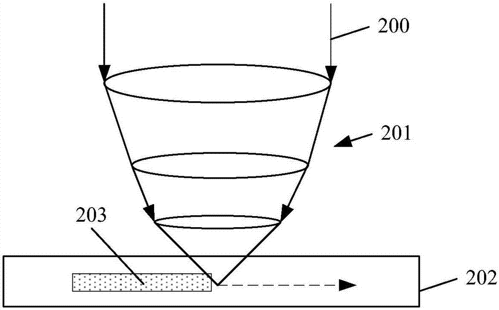
[0019] The specific implementation of the substrate localized amorphization method for nitride epitaxial growth provided by the present invention will be described in detail below with reference to the accompanying drawings.

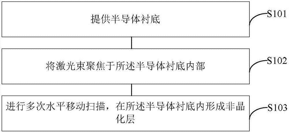
[0020] Please refer to figure 1 , is a schematic flowchart of a method for locally amorphizing a substrate according to a specific embodiment of the present invention.

[0021] The local amorphization method of the substrate includes:

[0022] Step S101: providing a semiconductor substrate.

[0023] The semiconductor substrate may be a semiconductor substrate such as a silicon substrate, a germanium substrate, or a silicon germanium substrate. In this specific implementation manner, the semiconductor substrate is a silicon substrate, such as a single crystal silicon wafer. The crystal orientation of the silicon substrate is . In other specific implementation manners of the present invention, the silicon substrate may also have other crystal orientati...


PUM

PropertyMeasurementUnit
Wavelengthaaaaaaaaaa
Spot diameteraaaaaaaaaa
Frequencyaaaaaaaaaa

Abstract

A local non-crystallization method of a substrate for epitaxial growth of a nitride comprises the steps of providing a semiconductor substrate; focusing a laser beam in the semiconductor substrate; and allowing the laser beam to be perpendicular to the semiconductor substrate, performing horizontal mobile scanning for many times, and forming a non-crystallization layer in the semiconductor substrate. According to the method, the non-crystallization layer is formed in the semiconductor substrate, and the semiconductor substrate can be used as a substrate for epitaxial growth of the nitride to form a high-quality nitride epitaxial layer.

Description

technical field [0001] The invention relates to the technical field of semiconductors, in particular to a method for local amorphization of a silicon substrate for nitride epitaxial growth. Background technique [0002] As a representative of wide-bandgap semiconductor materials, gallium nitride materials have great applications in optical display, storage, high-power, high-frequency electronic devices and other fields. In terms of optical performance, the emission wavelength of gallium nitride-based light-emitting diodes or lasers is tunable in the visible and even ultraviolet ranges. In terms of electrical characteristics, due to its advantages such as high breakdown electric field, wide band gap, high thermal conductivity, high electron mobility, and stable physical and chemical properties, gallium nitride is a high-frequency, high-efficiency, high-breakdown voltage, high-power Ideal material for electron mobility transistors (HEMTs). [0003] Due to the lack of homogen...

Claims


Application Information

Patent Timeline
IPC IPC(8): H01L21/02
CPCH01L21/02389H01L21/02658
Inventor 谢杰闫发旺张峰赵倍吉
Owner SHANGHAI SIMGUI TECH
Learn More