Full color OLED micro-display device manufacturing method

A technology for micro-display devices and display devices, which is applied in the manufacturing of semiconductor devices, electric solid-state devices, and semiconductor/solid-state devices, etc., can solve the problems of low product yield, wafer stress damage, and high resolution, and achieves improved productivity and good products. efficiency, reduce production costs, and improve resolution

Inactive Publication Date: 2017-07-04
ANHUI SEMICON INTEGRATED DISPLAY TECH CO LTD
View PDF8 Cites 15 Cited by
  • Summary
  • Abstract
  • Description
  • Claims
  • Application Information

AI Technical Summary

Problems solved by technology

The resolution of OLED microdisplay devices is high, the pixels are only a few microns in size, and the positioning accuracy of CCD is also about 1 μm, so the alignment is difficult, the accuracy is poor, and the problem of cross-color is prone to occur, which limits the improvement of device resolution
[0004] In addition, in the traditional manufacturing process of OLED microdisplay devices, the technology of first mechanical scribing and then bonding of small pieces of glass is adopted, and the process is complicated.
Mechanical scribing is the direct action of mechanical force on the wafer surface, causing stress damage inside the wafer. The heat-affected range and residual stress are large, easy to chip and break, and the product yield is low, which is not conducive to mass production.

Method used


Image

  • Full color OLED micro-display device manufacturing method

Examples


Embodiment 1

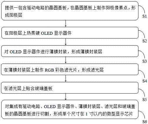
[0039] In the present embodiment, the production method of full-color OLED microdisplay device comprises the following steps:

[0040] A wafer substrate including a driving circuit is provided, and anode pixel points are fabricated on the wafer substrate to form an anode layer. The anode pixels are formed by evaporation, and the ambient vacuum is less than 10 -4 Pa, the material is selected from Cu. The OLED display device is thermally evaporated on the anode layer, and the OLED display device includes at least a light-emitting layer and a cathode layer, wherein the cathode layer is a semi-transparent structure; the OLED display device is thin-film encapsulated to form a thin-film encapsulation layer, the The thin film encapsulation layer is formed by alternately depositing multiple layers of organic or inorganic materials. The organic material of the thin film encapsulation layer is selected from polyacrylic acid, and the inorganic material is selected from Al 2 o 3 Making...

Embodiment 2

[0042] In the present embodiment, the production method of full-color OLED microdisplay device comprises the following steps:

[0043] A wafer substrate including a driving circuit is provided, and anode pixel points are fabricated on the wafer substrate to form an anode layer. The anode pixels are formed by evaporation, and the ambient vacuum is less than 10 -4 Pa, the material is selected from Al. An OLED display device is thermally evaporated on the anode layer, and the OLED display device at least includes a light-emitting layer and a cathode layer, wherein the cathode layer is a translucent structure. The OLED display device is encapsulated with a thin film to form a thin film encapsulation layer. The thin film encapsulation layer is formed by alternately depositing multiple layers of organic or inorganic materials. The organic material of the thin film encapsulation layer is selected from polyurethane acrylate, polyester, and the inorganic material is selected from from ...


PUM


Abstract

The invention discloses a full color OLED micro-display device manufacturing method, and the method comprises the following steps: a wafer substrate comprising a drive circuit is provided, anodic pixel points are manufactured on the wafer substrate, and an anode layer is formed; thermal evaporation is performed on an OLED display device on the anode layer; thin-film packaging is performed on the OLED display device, and a thin-film packaging layer; an RGB color filter is manufactured on the thin-film packaging layer, and a filter layer is formed; a glass cover plate fits the filter layer; the wafer substrate integrated with the drive circuit, the OLED display device, the thin-film packaging layer, the filter layer and the glass cover plate is cut, and a single micro-display chip within one inch is formed. According to the invention, the resolution ratio is improved, the manufacture cost of the device is reduced, and the productivity and the yield of the device are improved.

Description

technical field [0001] The invention relates to the production field of OLED microdisplay devices, in particular to a production method of full-color OLED microdisplay devices. Background technique [0002] Organic electroluminescent devices (OLEDs) have a series of advantages such as full solid state, self-luminescence, fast response speed, wide viewing angle, and wide operating temperature range, and have attracted more and more attention from academia and industry. After years of continuous active exploration, further optimization of the structure and process of the device and related materials, organic electroluminescence has made great progress, and has now achieved industrialization. According to the forecast of relevant research institutions, the output value of OLED panels will exceed 60 billion US dollars in 2020. OLED microdisplay refers to an organic light-emitting device driven by silicon-based CMOS with a display size of less than 1 inch. The pixel size is as h...

Claims


Application Information

Patent Timeline
Patent Type & Authority Applications(China)
IPC IPC(8): H01L51/56H01L27/32
CPCH10K59/38H10K71/00
Inventor 晋芳铭赵铮涛李文连任清江王仕伟
Owner ANHUI SEMICON INTEGRATED DISPLAY TECH CO LTD
Why Eureka
Try Eureka