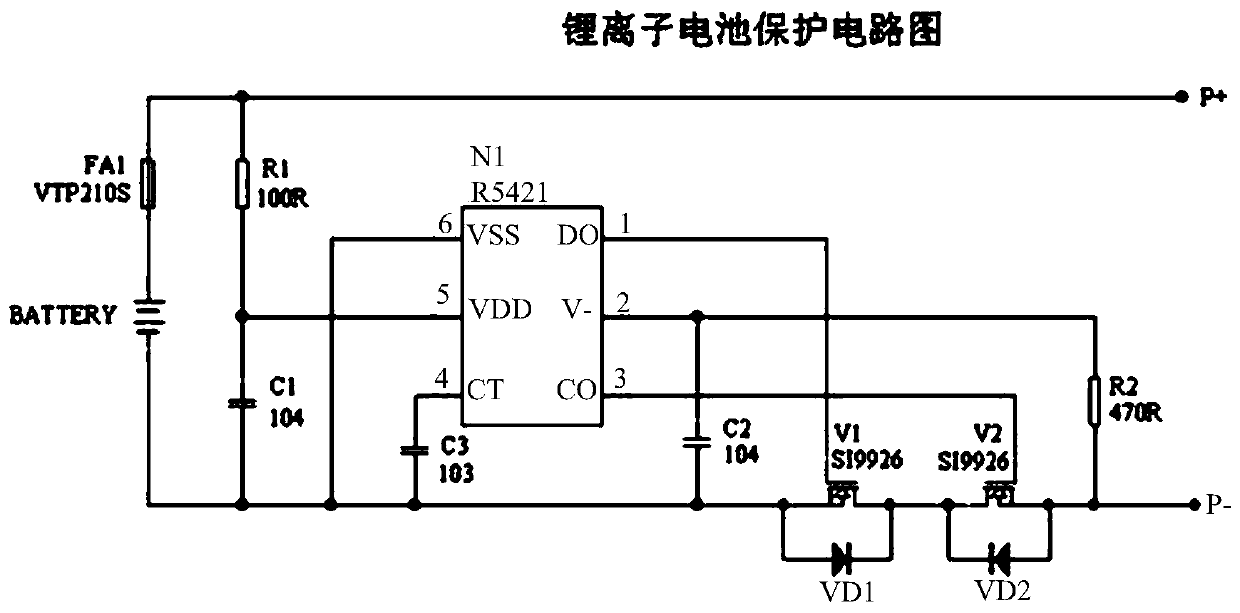
A switch device for lithium battery protection and manufacturing method thereof
A technology for switching devices and manufacturing methods, applied in semiconductor/solid-state device manufacturing, electrical components, semiconductor devices, etc., can solve the problems of large internal resistance and large area in the drift region of MOSFETs, and achieve low conduction internal resistance and reduced resistance , Guarantee the effect of constant pressure
- Summary
- Abstract
- Description
- Claims
- Application Information
AI Technical Summary
Problems solved by technology
Method used
Image
Examples
Embodiment 1
[0055] Such as Figure 2 to Figure 10 As shown, this embodiment provides a manufacturing method for a switching device for lithium battery protection, the manufacturing method includes steps:
[0056] Such as figure 2 As shown, step 1) is performed first, providing a P+ type substrate 101, and forming a P− type epitaxial layer 102 on the surface of the P+ type substrate 101.
[0057] Specifically, the doping concentration of the P+ type substrate 101 is 1e18-1e19 / cm 3 , using an epitaxial method to form a P-type epitaxial layer 102 on the surface of the P+ type substrate 101, and the doping concentration of the P-type epitaxial layer 102 is 1e16-1e17 / cm 3 .
[0058] Such as figure 2 As shown, then step 2) is performed to form an N-type well region 103 in the P-type epitaxial layer 102 .
[0059] Specifically, an N-type well region 103 is formed in the P-type epitaxial layer 102 by ion implantation without a mask, and the doping concentration of the N-type well region 10...
Embodiment 2
[0081] Such as Figure 12 As shown, this embodiment provides a method for manufacturing a switching device for lithium battery protection, the basic steps of which are as in Embodiment 1, wherein the difference from Embodiment 1 is that step 2) of this embodiment includes:
[0082] Step 2-1), making a mask on the P-type epitaxial layer 102;
[0083] In step 2-2), an N-type well region 103 is formed in the P-type epitaxial layer 102 by ion implantation based on a mask, so that the gap between the N-type well region 103 and the subsequently prepared body electrode 120 is covered. The P-type epitaxial layer 102 is isolated.
[0084] Such as Figure 12 As shown, this embodiment also provides a switching device for lithium battery protection, the basic structure of which is the same as that of Embodiment 1, wherein the difference from Embodiment 1 lies in: the N-type well region 103 and the body region The electrodes 120 are isolated by the P-type epitaxial layer 102 .
[0085]...
Embodiment 3
[0087] Such as Figure 13 As shown, this embodiment provides a method for manufacturing a switching device for lithium battery protection, the basic steps of which are as in embodiment 1, wherein the difference from embodiment 1 is that step 1) is also included in the P- The step of forming the STI isolation region 121 in the type epitaxial layer 102, the STI isolation region 121 is located between the two gate structures 104 fabricated subsequently, and the N-type drift region 106 prepared subsequently is surrounded by the STI isolation region 121 .
[0088] Such as Figure 13 As shown, this embodiment also provides a switching device for lithium battery protection, its basic structure is as in embodiment 1, wherein, the difference from embodiment 1 is that: the P-type epitaxial layer 102 is also formed with The STI isolation region 121 is located between the two gate structures 104 , and the N-type drift region 106 is surrounded by the STI isolation region 121 .
[0089] ...
PUM
 Abstract
Description
Claims
Application Information
 - R&D
- Intellectual Property
- Life Sciences
- Materials
- Tech Scout
- Unparalleled Data Quality
- Higher Quality Content
- 60% Fewer Hallucinations
Browse by: Latest US Patents, China's latest patents, Technical Efficacy Thesaurus, Application Domain, Technology Topic, Popular Technical Reports.
© 2025 PatSnap. All rights reserved.Legal|Privacy policy|Modern Slavery Act Transparency Statement|Sitemap|About US| Contact US: help@patsnap.com


