Novel plastic packaging structure for power MOS

A new type of high-power technology, applied in the manufacture of electrical components, electrical solid devices, semiconductor/solid devices, etc., can solve problems affecting product production efficiency, affecting device performance, and increasing device thermal resistance, so as to improve the safe working area and reduce Effect of package thermal resistance and low power consumption

Pending Publication Date: 2017-06-23
SHANGHAI CHANGYUAN WAYON MICROELECTRONICS
View PDF7 Cites 2 Cited by
  • Summary
  • Abstract
  • Description
  • Claims
  • Application Information

AI Technical Summary

Problems solved by technology

Generally, in order to simplify the process and better heat dissipation conditions, the chip 4' is pasted on the frame 1' by solder, and the back electrode (such as the drain of the power MOS) is directly connected to the back plate of the frame. The back electrode can pass through the middle The pins can also be connected to the external circuit through the backplane. The frame material is made of Cu with excellent thermal conductivity and electrical performance. If it is an in-line package, the backplane of the frame 1' needs to be soldered to the PCB board Add a heat sink, and the half-encapsulated package has an exposed backplane. In order to prevent short circuits, an insulating pad needs to be installed between the backplane and the heat sink. This will add a step to the process and affect the quality of the product. Production efficiency; in order to prevent this situation, when molding, the backplane of the frame can be completely wrapped with plastic molding compound to form a fully encapsulated package (Fullpak), which can avoid the use of insulating pads, but fully encapsulated devices Due to the poor thermal conductivity of the plastic encapsulation compound itself, the thermal resistance of the fully encapsulated device is doubled, which greatly affects the performance of the device. For power MOS, it also has a certain impact on the reliability of its UIS.

Method used


Image

  • Novel plastic packaging structure for power MOS
  • Novel plastic packaging structure for power MOS
  • Novel plastic packaging structure for power MOS

Examples


Embodiment Construction

[0027] In order to better understand the packaging structure, the present invention will be described in detail below in conjunction with the accompanying drawings and specific embodiments.

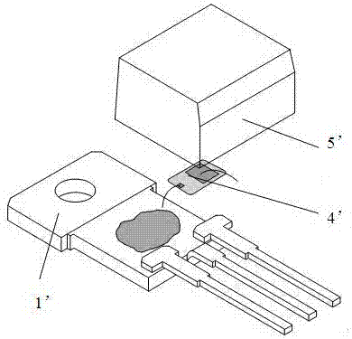
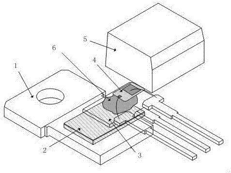
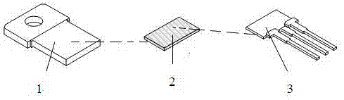
[0028] Such as Figure 2-4 As shown, a new type of plastic packaging structure suitable for power MOS includes a frame, a chip 2 and a package body, wherein the frame is a copper frame, and the copper frame is divided into two parts, one part is used as the carrier 3 and the device The back electrodes are connected and lead out pins to form an electrical connection, and a part is used to realize the heat dissipation backplane 1 of the heat dissipation function. The two are separated by a high thermal conductivity isolation layer, so that the two parts of the copper frame form a physical connection.

[0029] In this example, if Figure 4 As shown, the high thermal conductivity isolation layer adopts a ceramic isolation layer 2 covered with a copper layer on the upper and lower sides. The...


PUM


Abstract

The invention relates to a novel plastic packaging structure for a power MOS. The novel plastic packaging structure comprises a frame, a chip, and a packaging body. The frame is a copper frame having two parts; one part of the copper frame is used as a piece of slide glass and is connected with a back electrode of a device and a pin is led out to form electrical connection; and the other part of the copper frame is a cooling back panel for realizing a heat radiation function; and the two parts are isolated from each other by a high-thermal-conduction isolation layer, so that the two parts of the copper frame are in physical connection. According to the invention, because the slide glass and the cooling panel are independent parts isolated from each other and the slide glass is used for electrical connection and the cooling panel is used for providing a cooling channel, PCB assembling becomes convenient and the packaging thermal resistance of the power MOS can be reduced, and the security working zone at an application terminal is enhanced; and advantages of high power and low power consumption of the power MOS are fully realized.

Description

technical field [0001] The invention relates to a novel plastic encapsulation structure suitable for power MOS. Background technique [0002] As one of the main branches of power semiconductor devices, power field effect transistors (POWER MOS) are widely used in power supplies or adapters for consumer electronics such as mobile phones, computers, lighting and LCD TVs. Power MOS devices also have input impedance bottoms, Fast switching speed and other advantages. With the development of semiconductor technology, power MOS devices with high power, low power consumption and small package are attracting more and more people's attention. [0003] Power MOS devices are generally composed of many transistors with a cell structure connected in parallel. The structure and manufacturing process of the chip are the decisive factors for its performance quality, and further improvement of these technologies will pay a high cost. The package is a channel for communicating between the s...

Claims


Application Information

Patent Timeline
Patent Type & Authority Applications(China)
IPC IPC(8): H01L21/48H01L21/56H01L23/495
CPCH01L21/4882H01L21/56H01L23/49513H01L23/49568H01L2224/83192H01L2224/32245H01L2224/73265
Inventor 任杰苏海伟
Owner SHANGHAI CHANGYUAN WAYON MICROELECTRONICS
Why Eureka
Try Eureka