A kind of translucent organic metal halide perovskite thin film solar cell and its preparation method
A halide perovskite and solar cell technology, applied in the field of solar cells, can solve the problems of low photoelectric conversion efficiency and low surface flatness of perovskite solar cells, and achieve improved photoelectric conversion efficiency, obvious film-forming performance, The effect of grain boundary reduction
- Summary
- Abstract
- Description
- Claims
- Application Information
AI Technical Summary
Problems solved by technology
Method used
Image
Examples
Embodiment 1
[0033] In comparative example 1 step 4, except PbI 2 and CH 3 NH 3 I joins in the mixed solvent of DMF and DMSO, also adds a certain amount of PVdF-HFP (M W =400000, commercially available), so that its concentration was 5 mg / mL. All the other steps are the same as in Comparative Example 1.
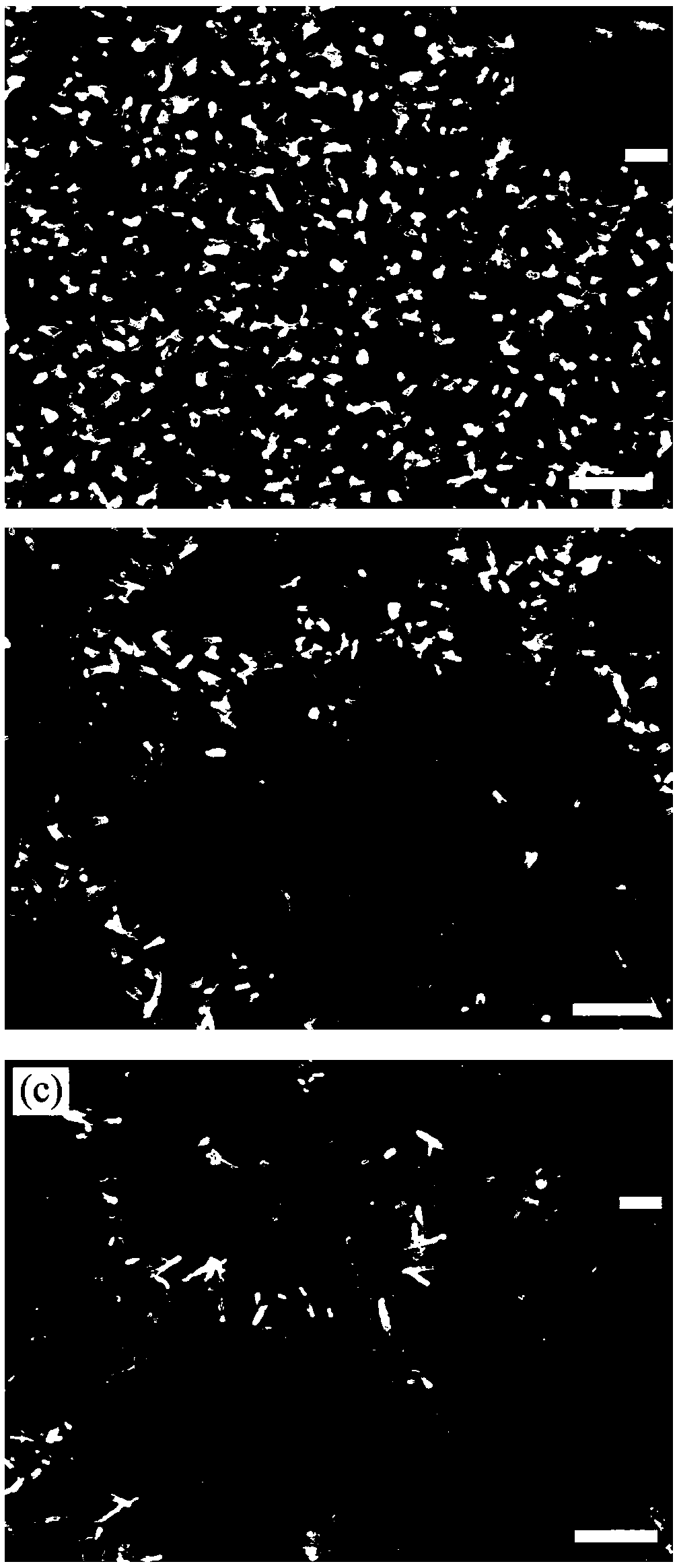
[0034] To the FTO / TiO obtained in embodiment 1 2 / Perovskite structure was characterized by SEM. Its surface SEM figure shows that the perovskite thin film pinhole reduces compared with Comparative Example 1 ( figure 1 b). The I-V curve (under simulated sunlight of AM 1.5G) was tested on the obtained semi-transparent cell, and its efficiency was 8.9% (higher than that of Comparative Example 1).
Embodiment 2
[0036] In Example 1, the concentration of PVdF-HFP in the perovskite precursor solution was adjusted to 12 mg / mL. All the other steps are the same as in Example 1.
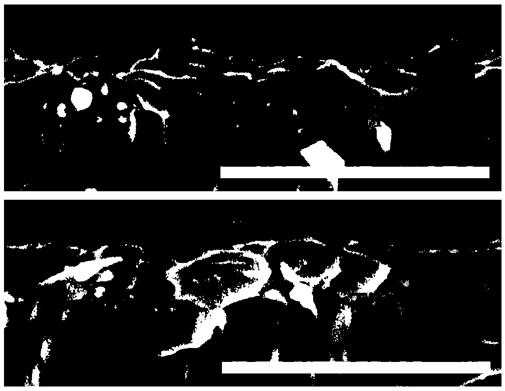
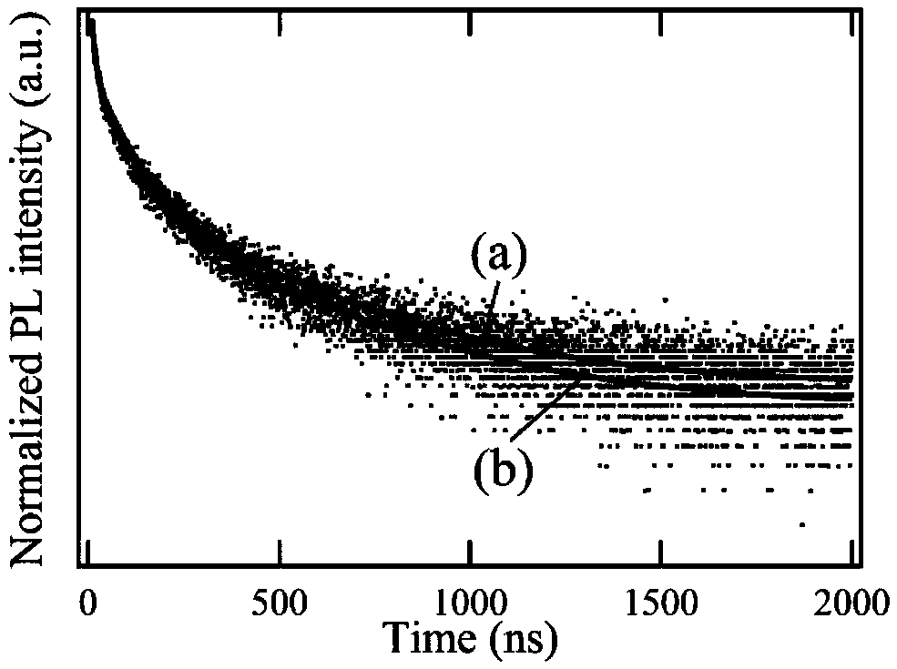
[0037] To the FTO / TiO obtained in embodiment 2 2 / Perovskite structure was characterized by SEM. Its surface SEM figure shows that the pinholes of the perovskite film are further reduced than in Example 1, the grain boundaries become blurred, and the grains increase ( figure 1 c), the cross-sectional SEM image shows that the perovskite film has high flatness and a thickness of about 150nm ( figure 2 b). The perovskite thin films obtained in comparative example 1 and the present embodiment were characterized by transient fluorescence, and it was found that the fluorescence lifetime of the perovskite thin films of the present embodiment was higher than that of comparative example 1 ( image 3 ). The I-V curve test (under the simulated sunlight of AM 1.5G) was carried out on the obtained translucent cell, and ...
Embodiment 3
[0039] PbI in the perovskite precursor solution 2 and CH 3 NH 3 The concentration of I was adjusted to 0.25mol / L, and the spin coating conditions of the perovskite precursor solution were changed to: 1000rpm / min for 10s in the first stage, and 7000rpm / min for 55s in the second stage. All the other steps are the same as in Example 2.
[0040] To the FTO / TiO obtained in embodiment 3 2 / The perovskite structure was characterized by SEM, and it was found that the pinholes of the perovskite film were reduced compared with Comparative Example 2, the surface smoothness was good, and the thickness was about 30nm. The I-V curve (under simulated sunlight of AM1.5G) was tested on the obtained semi-transparent cell, and its efficiency was 2.3% (higher than that of Comparative Example 2).
PUM
 Abstract
Description
Claims
Application Information
 - R&D
- Intellectual Property
- Life Sciences
- Materials
- Tech Scout
- Unparalleled Data Quality
- Higher Quality Content
- 60% Fewer Hallucinations
Browse by: Latest US Patents, China's latest patents, Technical Efficacy Thesaurus, Application Domain, Technology Topic, Popular Technical Reports.
© 2025 PatSnap. All rights reserved.Legal|Privacy policy|Modern Slavery Act Transparency Statement|Sitemap|About US| Contact US: help@patsnap.com


