
Etching mask and method for manufacturing LED by aid of same

A manufacturing method and a mask technology, which are applied in the direction of originals for photomechanical processing, photoplate-making process of patterned surface, instruments, etc., can solve the problems of prolonging the production cycle and increasing the production cost of LEDs, and achieve saving of production costs, The production process is convenient and fast

Active Publication Date: 2017-05-31
ANHUI SANAN OPTOELECTRONICS CO LTD
View PDF2 Cites 2 Cited by
  • Summary
  • Abstract
  • Description
  • Claims
  • Application Information

AI Technical Summary

Problems solved by technology

Due to the gluing, exposure, and development steps in the photolithography method, the LED manufacturing cost is increased and the manufacturing cycle is prolonged. Therefore, it is necessary to make necessary improvements to the LED manufacturing method

Method used


Image

  • Etching mask and method for manufacturing LED by aid of same
  • Etching mask and method for manufacturing LED by aid of same
  • Etching mask and method for manufacturing LED by aid of same

Examples


Embodiment Construction

[0029] In the following paragraphs the invention is described more specifically by way of example with reference to the accompanying drawings. Advantages and features of the present invention will be apparent from the following description and claims. It should be noted that all the drawings are in a very simplified form and use imprecise scales, and are only used to facilitate and clearly assist the purpose of illustrating the embodiments of the present invention.

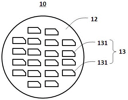
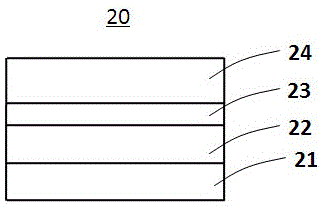
[0030] figure 1 with figure 2 An etching mask 10 (hereinafter simply referred to as "mask") of the present invention is shown. It can be observed from the side schematic diagram of the mask 10 that the mask 10 includes three layers from bottom to top, which are respectively a first flexible substrate 11, a first adhesive layer 12 and a patterned structure layer 13, and the patterned structure layer 13 It is closely bonded to the first flexible substrate 11 through the first adhesive layer 12 . The patterned s...


PUM


Abstract

The invention belongs to the field of processes for manufacturing semiconductors, and relates to an etching mask and a method for manufacturing an LED by the aid of the same. The etching mask comprises a first flexible substrate, a first adhesion layer and a patterned structural layer. The first flexible substrate, the first adhesion layer and the patterned structural layer are sequentially lapped on one another and are closely adhered with one another. The method includes arranging the etching mask on the surface of an epitaxial wafer; transferring patterns of the patterned structural layer onto the epitaxial wafer by means of dry etching; manufacturing a patterned epitaxial wafer. The etching mask and the method have the advantages that the etching mash and the method are convenient and speedy, and the cost can be saved; a second adhesion layer and a second flexible substrate can be adhered on the patterned structural layer after the patterned structural layer is subjected to dry etching, the patterned structural layer can be peeled off to form an etching mask again, and accordingly the etching mask can be recycled.

Description

technical field [0001] The invention belongs to the field of semiconductor manufacturing, and in particular relates to a reusable etching mask and a method for manufacturing LEDs by using the etching mask. Background technique [0002] At present, in the manufacturing process of LEDs, it is necessary to use photolithography many times to form desired patterns. Photolithography, where a resist (such as photoresist) is first applied to the epitaxial wafer and then the resist is exposed. Thereafter, a resist mask is formed by dissolving the exposed portion of the resist of a predetermined pattern in a developer (positive type), or by making the resist portion difficult to dissolve (negative type), and is etched by etching (e.g. dry etching and wet etching) the epitaxial wafer, forming a pattern with etched and unetched portions, transferring the pattern of the resist mask to the epitaxial wafer. Since the steps of gluing, exposure, and development in the photolithography meth...

Claims


Application Information

Patent Timeline
Patent Type & Authority Applications(China)
IPC IPC(8): H01L33/00G03F1/00
CPCG03F1/00H01L33/005
Inventor 蔡家豪吴和兵陈明皓马建华孙京京魏峰邱智中张家宏
Owner ANHUI SANAN OPTOELECTRONICS CO LTD
Learn More