
Anti-emi super junction vdmos device structure and its preparation method

A device structure, deep trench technology, applied in semiconductor/solid-state device manufacturing, semiconductor devices, electric solid-state devices, etc., can solve problems such as high doping concentration, serious EMI problems, and EMI at the input and output ends of the circuit system , to achieve the effect of improving the EMI problem

Active Publication Date: 2019-11-15
XIAN LONTEN RENEWABLE ENERGY TECH
View PDF5 Cites 0 Cited by
  • Summary
  • Abstract
  • Description
  • Claims
  • Application Information

AI Technical Summary

Problems solved by technology

The sharp change in the capacitance of the power device will cause a sharp change in the voltage or current on the drain and gate sides of the power device, which will be superimposed on the electronic circuit and cause EMI problems at the input and output ends of the circuit system.
[0004] With the advancement of deep trench epitaxial filling technology, the cell density of super junction VDMOS is getting higher and higher, the doping concentration of N-type epitaxial region is getting higher and higher, and the trench spacing is getting smaller and smaller. Reduce the on-resistance R ds(on) At the same time, it can meet the requirements of the breakdown voltage BV, and the trench depth is correspondingly deeper and deeper, but this also brings a problem that the deeper the trench, the more serious the EMI problem caused by power devices.

Method used


Image

  • Anti-emi super junction vdmos device structure and its preparation method
  • Anti-emi super junction vdmos device structure and its preparation method
  • Anti-emi super junction vdmos device structure and its preparation method

Examples


Embodiment Construction

[0032] The present invention will be described in detail below in combination with specific embodiments.

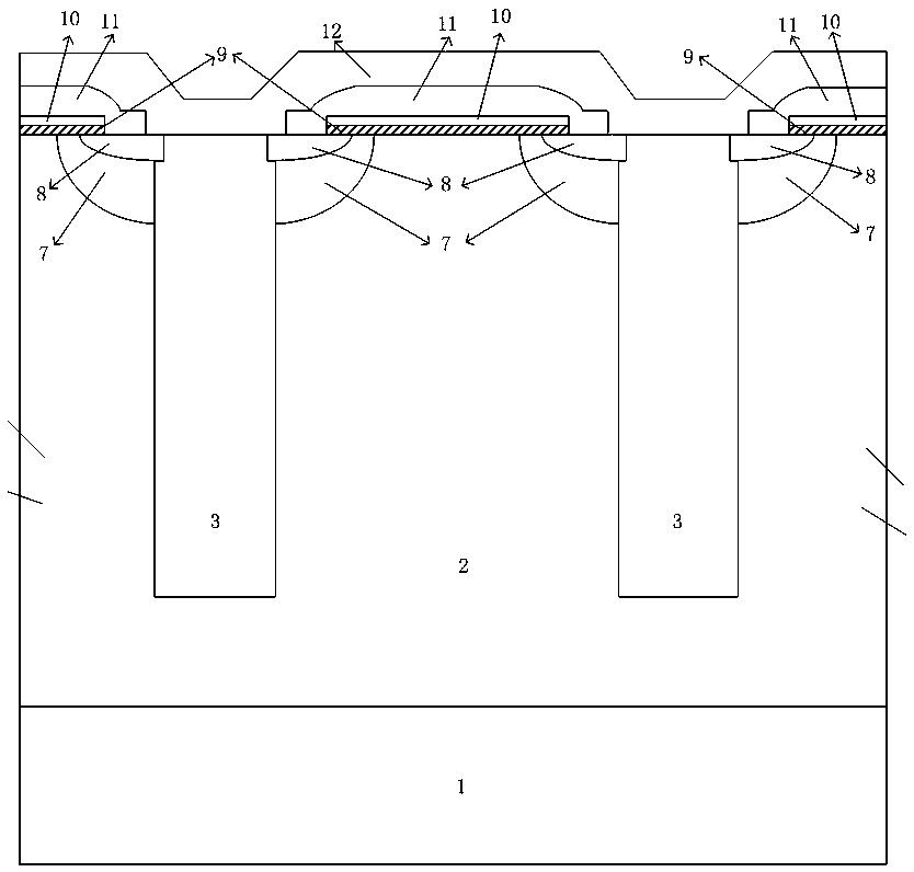
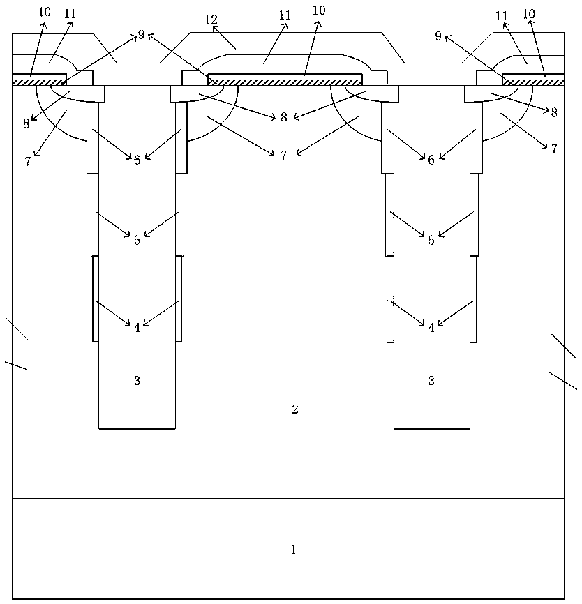
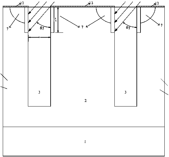
[0033] The invention relates to a method for manufacturing an EMI-resistant superjunction VDMOS device. In the process of manufacturing superjunction using deep trench epitaxial filling technology, after etching the deep trench, three times of boron ion implantation with different inclination angles are used in sequence. A P-type auxiliary depletion first region 6 , a P-type auxiliary depletion second region 5 and a P-type auxiliary depletion third region 4 are formed. Specifically, it is realized through the following steps:

[0034] Step 1. Using the epitaxial process, the heavily doped N + An N-type epitaxial layer 2 of 35-50 μm is epitaxially grown on the substrate 1;

[0035] Step 2: Perform boron ion implantation on the N-type epitaxial layer 2 through the Pbody photolithography mask, and push the junction at a high temperature of 900-1200°C for 90-300 minutes to ...


PUM


Abstract

The invention relates to an anti-EMI super-junction VDMOS device structure and a preparation method thereof. The method is characterized by carrying out boron ion implantation for three times at different inclination angles to form three P-type auxiliary depletion regions respectively after etching a deep trench in the process of preparing a super junction through a deep trench epitaxial filling technique, so that change of capacitance and Miller capacitance between a drain electrode and a source electrode caused at the moment a superjunction VDMOS is turned on or turned off can be slowed, and electronic system EMI characteristics are improved.

Description

technical field [0001] The invention belongs to the technical field of semiconductor power devices, and in particular relates to an anti-EMI super junction VDMOS device structure and a preparation method thereof. Background technique [0002] In applications such as high-voltage switching power supplies, vertical double-diffused metal-oxide-semiconductor field-effect transistors (VDMOS) with good body diode characteristics and high durability are required. However, conventional planar VDMOS devices have relatively high on-resistance, resulting in relatively high conduction losses in electronic systems. In the late 1990s, super-junction VDMOS devices designed based on the charge balance concept of the super-junction theory (Super-Junction) were introduced into the market. Compared with the conventional high-voltage planar VDMOS, the on-resistance Rsp per unit area of ​​the super-junction VDMOS is much smaller, so the super-junction VDMOS has a much smaller on-resistance Rds(...

Claims


Application Information

Patent Timeline
Patent Type & Authority Patents(China)
IPC IPC(8): H01L21/336H01L23/552H01L29/06H01L29/78
CPCH01L23/552H01L29/0634H01L29/66712H01L29/7802
Inventor 任文珍周宏伟张园园徐西昌
Owner XIAN LONTEN RENEWABLE ENERGY TECH
Learn More