Vertical-channel SiC junction gate bipolar transistor and preparation method thereof
A bipolar transistor and junction gate technology, applied in the field of microelectronics, can solve the problems of complex structure, low production cost and yield, and reduce device mobility, so as to avoid the influence of device characteristics and reduce the difficulty of device technology Effect
- Summary
- Abstract
- Description
- Claims
- Application Information
AI Technical Summary
Problems solved by technology
Method used
Image
Examples
Embodiment 1
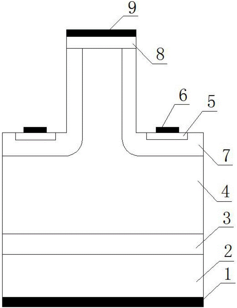
[0046] A SiC junction gate bipolar transistor device with a vertical channel, specifically as figure 2 As shown, including an N+ silicon carbide substrate 2, an emitter contact metal layer 1 formed on the surface of the N+ silicon carbide substrate 2, a P+ buffer layer 3 formed on the N+ silicon carbide substrate 2, and a P+ buffer layer 3 formed on the P-drift region 4, P+ collector region 8 formed on P-drift region 4, collector contact metal layer 9 formed on P+ collector region 8; also includes at least two P+ collector regions formed on P-drift region 4 a vertical trench, the bottom of the trench and the side walls of the trench are provided with an N-type gate region 7, the N-type gate region 7 at the bottom of the trench is implanted with a gate N+ implantation region 5, and the gate N+ implantation region 5 is formed with a The gate is in contact with the metal layer 6 ; the N-type gate region 7 is in contact with the P+ collector region 8 .
[0047] Among them, the e...
Embodiment 2
[0075] A SiC junction gate bipolar transistor device with a vertical channel, specifically as figure 2 As shown, including an N+ silicon carbide substrate 2, an emitter contact metal layer 1 formed on the surface of the N+ silicon carbide substrate 2, a P+ buffer layer 3 formed on the N+ silicon carbide substrate 2, and a P+ buffer layer 3 formed on the P-drift region 4, P+ collector region 8 formed on P-drift region 4, collector contact metal layer 9 formed on P+ collector region 8; also includes at least two P+ collector regions formed on P-drift region 4 a vertical trench, the bottom of the trench and the side walls of the trench are provided with an N-type gate region 7, the N-type gate region 7 at the bottom of the trench is implanted with a gate N+ implantation region 5, and the gate N+ implantation region 5 is formed with a The gate is in contact with the metal layer 6 ; the N-type gate region 7 is in contact with the P+ collector region 8 .
[0076] Among them, the e...
Embodiment 3
[0104] A SiC junction gate bipolar transistor device with a vertical channel, specifically as figure 2 As shown, including an N+ silicon carbide substrate 2, an emitter contact metal layer 1 formed on the surface of the N+ silicon carbide substrate 2, a P+ buffer layer 3 formed on the N+ silicon carbide substrate 2, and a P+ buffer layer 3 formed on the P-drift region 4, P+ collector region 8 formed on P-drift region 4, collector contact metal layer 9 formed on P+ collector region 8; also includes at least two P+ collector regions formed on P-drift region 4 a vertical trench, the bottom of the trench and the side walls of the trench are provided with an N-type gate region 7, the N-type gate region 7 at the bottom of the trench is implanted with a gate N+ implantation region 5, and the gate N+ implantation region 5 is formed with a The gate is in contact with the metal layer 6 ; the N-type gate region 7 is in contact with the P+ collector region 8 .
[0105] Among them, the e...
PUM
| Property | Measurement | Unit |
|---|---|---|
| width | aaaaa | aaaaa |
| thickness | aaaaa | aaaaa |
| thickness | aaaaa | aaaaa |
Abstract
Description
Claims
Application Information
 - Generate Ideas
- Intellectual Property
- Life Sciences
- Materials
- Tech Scout
- Unparalleled Data Quality
- Higher Quality Content
- 60% Fewer Hallucinations
Browse by: Latest US Patents, China's latest patents, Technical Efficacy Thesaurus, Application Domain, Technology Topic, Popular Technical Reports.
© 2025 PatSnap. All rights reserved.Legal|Privacy policy|Modern Slavery Act Transparency Statement|Sitemap|About US| Contact US: help@patsnap.com


